HomeTag

via transition - KKPCB

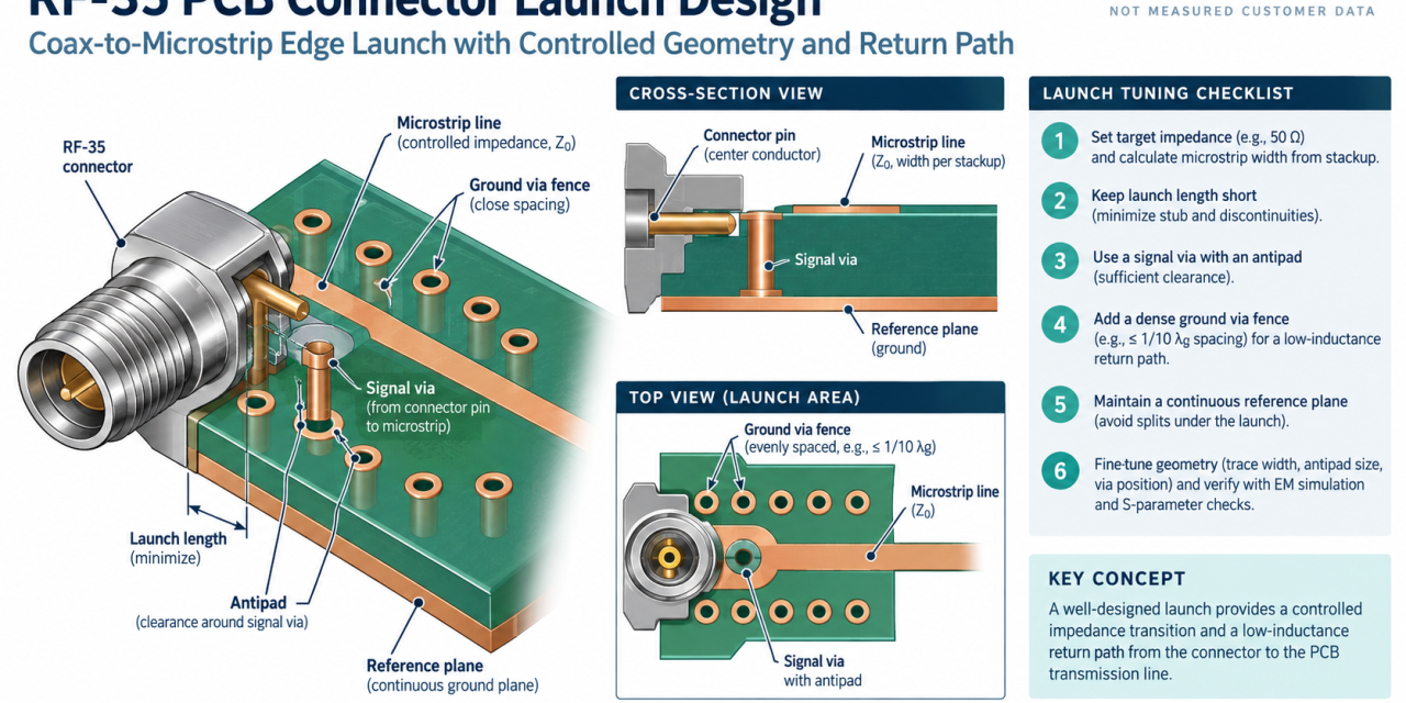
RF-35 PCB Connector Launch and Via Transition: A Practical Verification Workflow

A connector launch is the shortest and most fragile transmission-line section on many microwave boards. The signal leaves a coaxial pin, crosses a pad and via, and then enters a controlled planar line. This guide uses an RF-35 PCB example to show how to release that transition with a defined return path, manufacturable clearances, and...
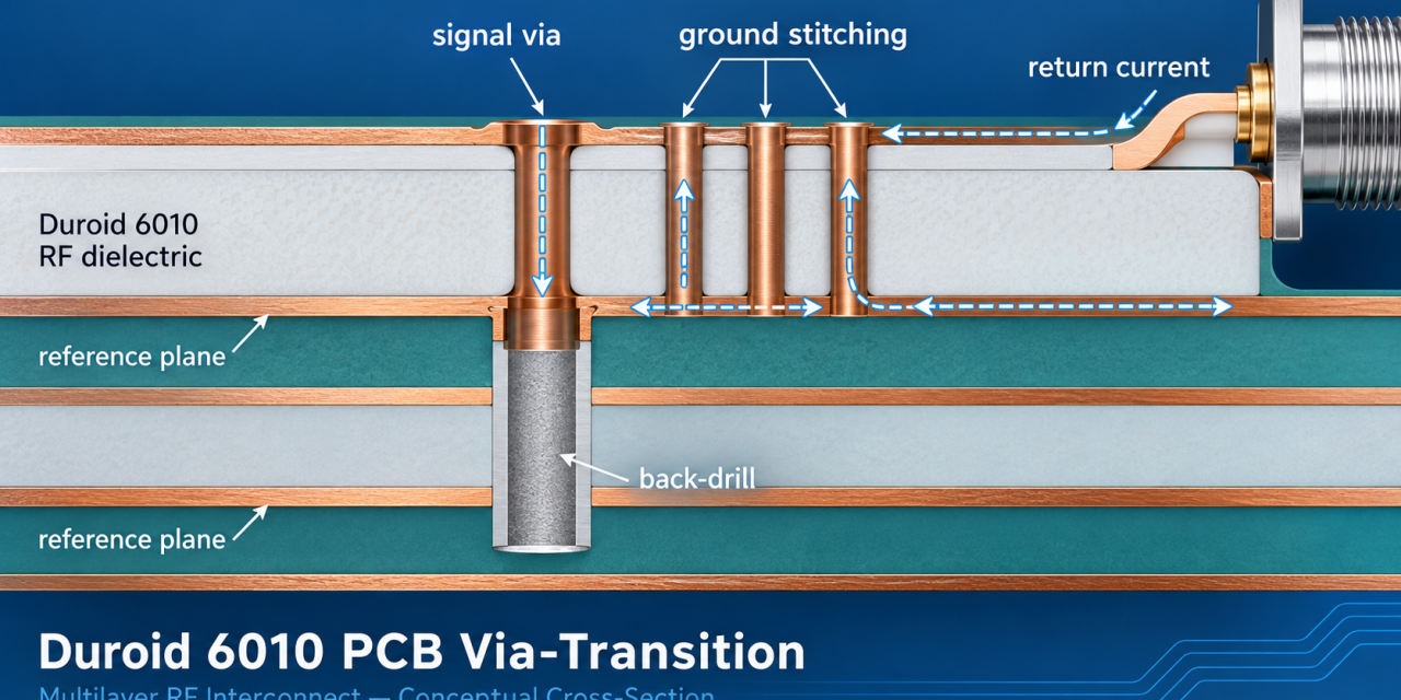
Duroid 6010 PCB Via Transition: 7 Critical Controls for Stable RF Interconnects

Table of Contents Why via transitions become the RF bottleneck Seven controls for a stable interconnect Return path and back-drill Launch and inspection evidence Release checklist A Duroid 6010 PCB via transition can dominate microwave performance when the signal changes layers, connects to a board-edge launch, or crosses a split reference plane. The project pain...

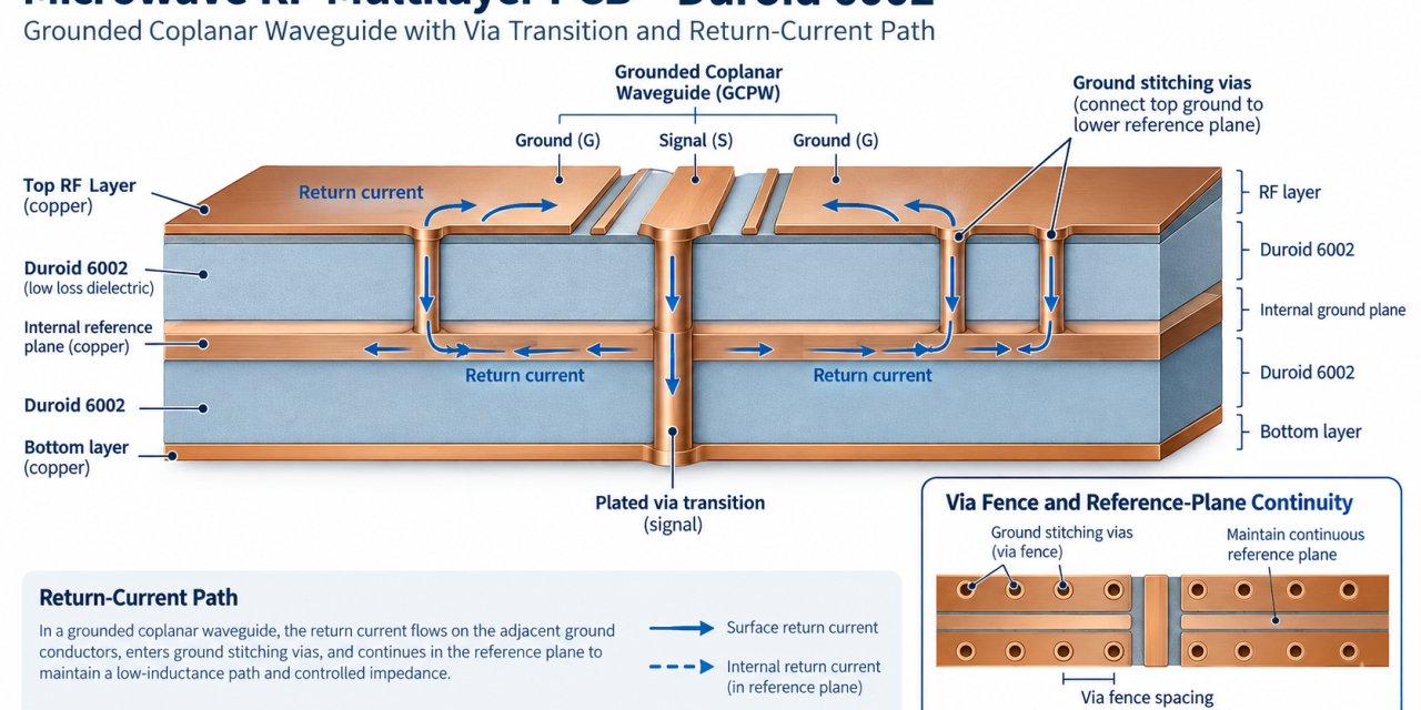
Duroid 6002 PCB Via Transition: 7 Critical Controls for Stable Microwave Return Paths

Table of Contents Why via transitions fail in production Seven controls for a stable return path Reference planes and geometry Drilling, plating, and launch details Inspection and release checklist A Duroid 6002 PCB is often chosen for low-loss microwave paths, yet many projects still lose margin at the via transition. The practical problem is rarely...

Hybrid Stackup Design Using Duroid 6010 PCB for High-Density RF and Microwave Packaging

Advanced RF Packaging Requires Hybrid PCB Stackup Technology As modern RF and microwave systems continue evolving toward: 5G and 6G communication millimeter-wave radar satellite communication aerospace RF electronics defense microwave systems high-density RF modules advanced phased-array antennas the demand for: higher integration density lower signal loss stable impedance control compact RF packaging has increased dramatically....