
A connector launch is the shortest and most fragile transmission-line section on many microwave boards. The signal leaves a coaxial pin, crosses a pad and via, and then enters a controlled planar line. This guide uses an RF-35 PCB example to show how to release that transition with a defined return path, manufacturable clearances, and a verification coupon.
RF-35 is a ceramic-filled PTFE/glass laminate family used for RF and microwave designs. Supplier typical tables list Dk near 3.50 at 1.9 GHz and a low dissipation factor, but the approved material revision and finished stackup remain the source of truth. Do not treat the values in a marketing graphic or calculator as measured data for a customer board.
1. Map the RF-35 PCB launch interface
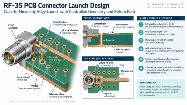
The first step is to mark every reference plane that the field sees from connector pin to transmission line. A microstrip launch needs a continuous plane beneath the signal. A grounded coplanar launch also depends on side grounds and a via fence. If the reference plane is split, necked down, or interrupted by an antipad, the launch impedance can change before the signal reaches the main route.
- Record connector part number, pin diameter, pad finish, and allowable launch length.
- Assign a target impedance and tolerance to the launch net class.
- Show the ground-via fence, antipad, and plane clearance in the footprint.
- Identify whether the transition uses a through, blind, buried, or back-drilled via.
A high-frequency PCB review should look at the complete electromagnetic path. A trace-width-only review can miss the inductance of a long pin, the capacitance of an oversized pad, or the return-current detour around a keepout.
2. Control launch geometry in the stackup
For an RF-35 PCB, launch geometry should be calculated from the pressed dielectric height and finished copper state. Define the pad diameter, trace width, gap to side ground, via capture pad, antipad diameter, and connector pin overlap as one structure. If any item changes, rerun the model and update the drawing rather than adjusting only the trace width.
Practical geometry controls
| Feature | Typical design question | Release note |
|---|---|---|
| Launch pad | Does the pad add excess shunt capacitance? | Keep diameter and solder-mask opening tied to the connector drawing. |
| Signal via | Is the barrel long enough to create a stub? | Specify finished drill, pad, antipad, and back-drill option. |
| Ground vias | Does the return path stay close to the signal? | Control pitch, distance, and layer connection in the footprint. |
| Reference plane | Is copper continuous beneath the launch? | Keep voids and splits outside the current path. |
Use a controlled PCB design model with the supplier’s approved Dk assumption. Glass style, resin content, and pressed thickness influence the effective field, so a generic 50-ohm footprint cannot be copied between every RF-35 PCB stack.
3. Manage via transitions and return paths
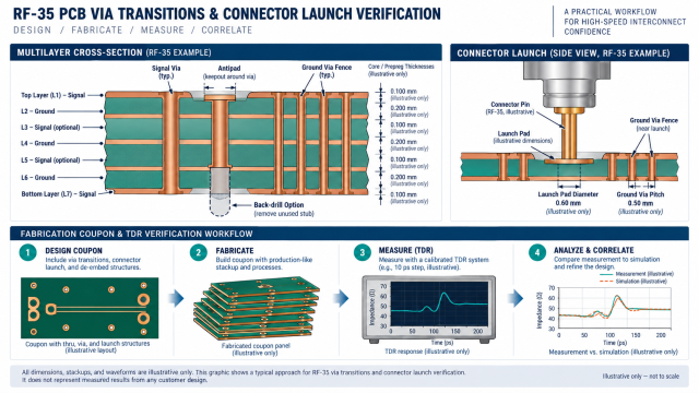
Via transitions are often where a good launch becomes a lossy or reflective launch. A long through-via carries a signal past several reference planes; each unused section behaves as a stub. A back-drill, blind via, or alternate layer transition can reduce the unused barrel, but the decision must follow the real board thickness and the fabricator’s drill process.
On an RF-35 PCB, the via fence should connect the intended ground layers without creating an accidental resonant cavity. Leave enough annular ring for registration and plating, and keep the antipad large enough to meet the modeled clearance after drill tolerance. If a mounting hole, shield wall, or test pad interrupts the fence, document the local return-path exception.
4. Verify with a representative coupon
A coupon for an RF-35 PCB should reproduce the critical layer pair, plated-hole class, copper treatment, and launch geometry. Use it to support microsection review, dimensional checks, and an agreed TDR or fixture measurement. Label any plotted waveform as illustrative until it is generated from a calibrated instrument and an identified production coupon.
The released acceptance plan should define reference-plane continuity, launch dimensions, via registration, and the impedance window. A PCB manufacturing traveler should point to the same revision-controlled drawing. KKPCB can review the stackup and propose a buildable drill sequence before panel tooling is released.
5. Release the assembly package
The connector is also an assembly feature. Provide the PCB assembly team with the approved paste aperture, solder-mask opening, connector seating direction, torque or press-fit notes, and any no-rework zone around the launch. Excess solder or an unplanned mask web can add capacitance and alter the transition.
For demanding multilayer work, KKPCB states capability up to 62 layers and 8 sequential lamination steps. That capability supports physical separation between RF, digital, and power structures, but the launch still needs a realistic panel outline, registration budget, and inspection access. In summary, the most reliable RF-35 PCB launch is one that is modeled, drawn, fabricated, inspected, and assembled as a single interface.
Sources: Taconic RF-35 and RF-35P processing guidance and typical property tables; IPC-TM-650 references for impedance and microsection evaluation; and KKPCB manufacturing capability notes. Typical values are reference data rather than customer measurements; verify the current supplier datasheet and lot before release.
