HomeTag

via transition - KKPCB

Ku/Ka Satellite PCB Launch Design: Taming Connector and Via Transitions at 30 GHz

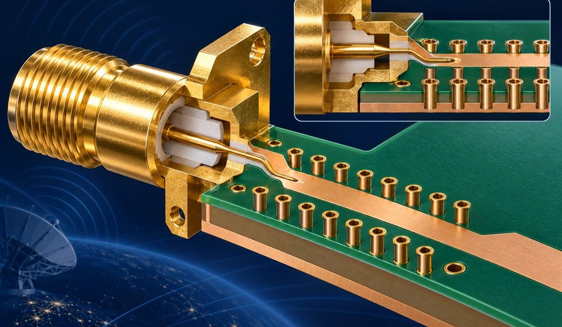
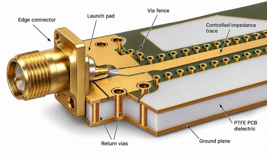
For Satellite PCB launch design, a Ku/Ka payload can meet its schematic targets and still lose margin at the board edge. The connector, launch pad, reference plane, via field, and enclosure datum form one electromagnetic interface. The Satellite PCB release must hold that board-to-enclosure datum constant across design and manufacturing. At 30 GHz, even a...
Megtron 7 PCB Connector Launches: A Back-Drill and Ground-Return Review for Multi-Gigabit Ports

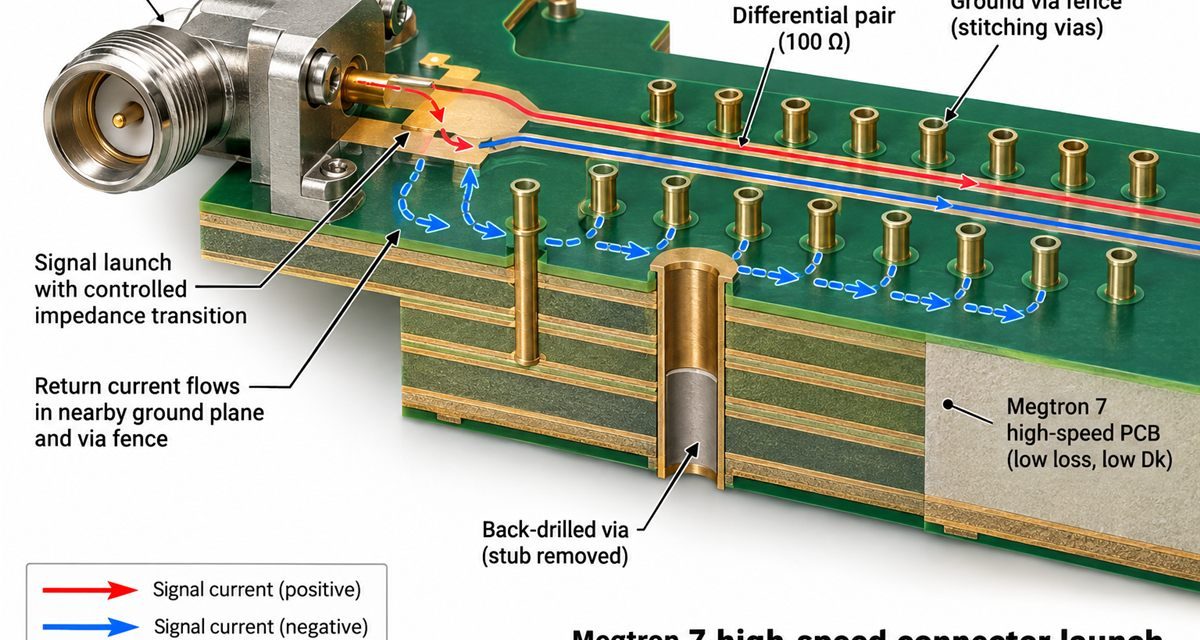
Connector launches often become the hidden bottleneck in a high-speed program. The laminate may have a low loss tangent, but an unused barrel stub, a broken reference plane, or an asymmetric ground-via pattern can dominate the transition. Treat every Megtron 7 PCB as a small RF structure with its own geometry, datum, and verification plan....

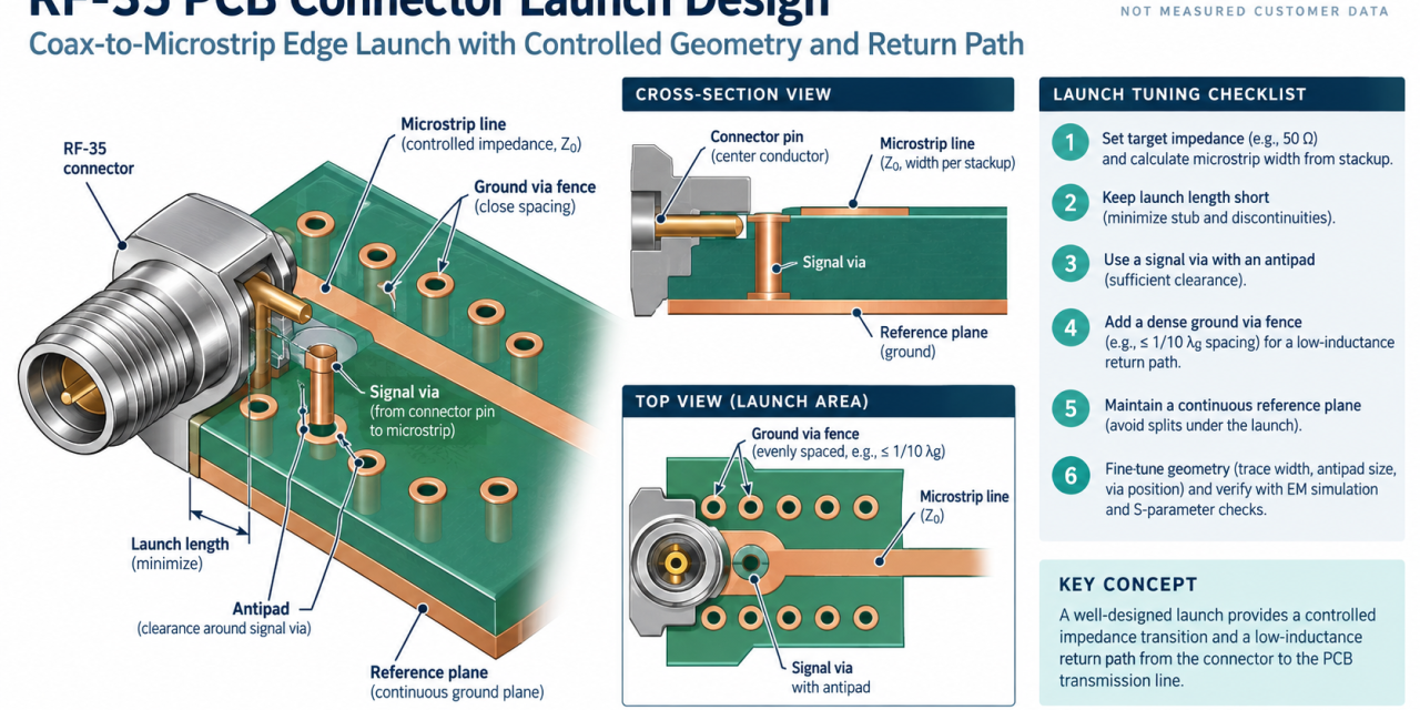
RF-35 PCB Connector Launch and Via Transition: A Practical Verification Workflow

A connector launch is the shortest and most fragile transmission-line section on many microwave boards. The signal leaves a coaxial pin, crosses a pad and via, and then enters a controlled planar line. This guide uses an RF-35 PCB example to show how to release that transition with a defined return path, manufacturable clearances, and...

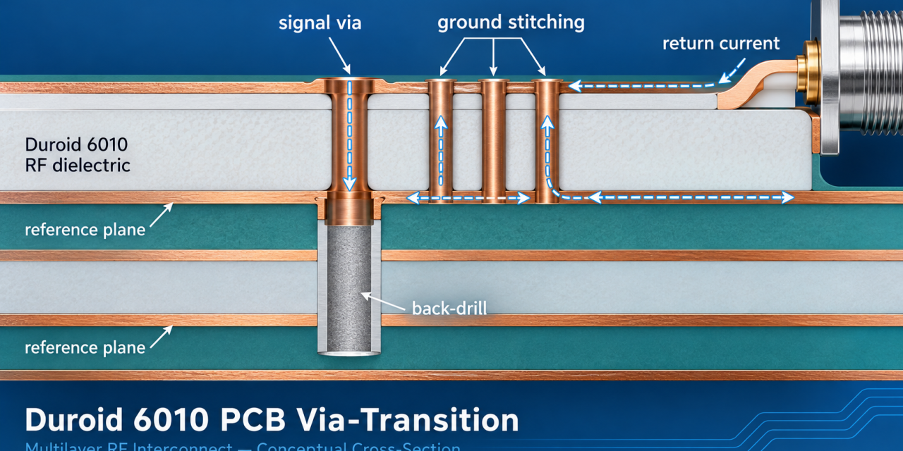
Duroid 6010 PCB Via Transition: 7 Critical Controls for Stable RF Interconnects

Table of Contents Why via transitions become the RF bottleneck Seven controls for a stable interconnect Return path and back-drill Launch and inspection evidence Release checklist A Duroid 6010 PCB via transition can dominate microwave performance when the signal changes layers, connects to a board-edge launch, or crosses a split reference plane. The project pain...

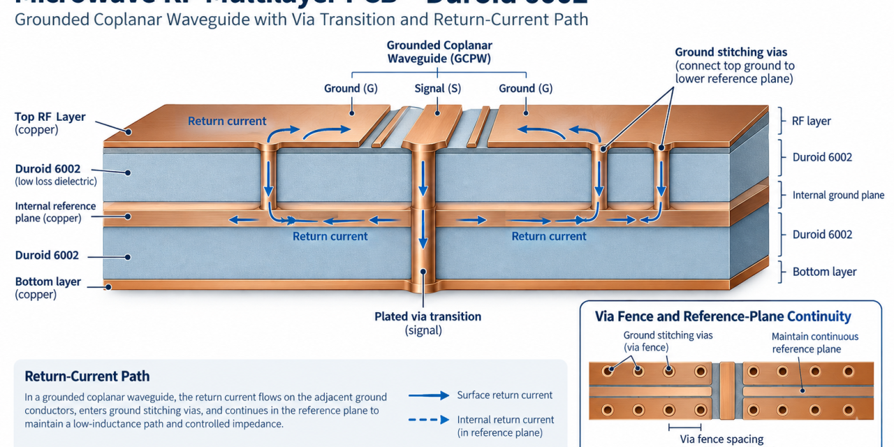
Duroid 6002 PCB Via Transition: 7 Critical Controls for Stable Microwave Return Paths

Table of Contents Why via transitions fail in production Seven controls for a stable return path Reference planes and geometry Drilling, plating, and launch details Inspection and release checklist A Duroid 6002 PCB is often chosen for low-loss microwave paths, yet many projects still lose margin at the via transition. The practical problem is rarely...

Hybrid Stackup Design Using Duroid 6010 PCB for High-Density RF and Microwave Packaging

Advanced RF Packaging Requires Hybrid PCB Stackup Technology As modern RF and microwave systems continue evolving toward: 5G and 6G communication millimeter-wave radar satellite communication aerospace RF electronics defense microwave systems high-density RF modules advanced phased-array antennas the demand for: higher integration density lower signal loss stable impedance control compact RF packaging has increased dramatically....