1. Introduction: Why Megtron 7 PCB Technology Is Important
Modern high-speed electronic systems continue advancing toward:
- Higher data transmission rates
- AI-driven computing infrastructure
- 800G and higher networking systems
- Advanced cloud computing platforms
- Ultra-high-speed communication architectures
Applications such as:
- AI servers
- Data centers
- 5G and 6G communication systems
- High-performance networking equipment
- High-speed switching platforms
require PCB materials capable of delivering:
- Ultra-low transmission loss
- Excellent signal integrity
- Stable controlled impedance
- High thermal reliability
Traditional FR4 PCB materials often struggle with:
- Excessive dielectric loss
- Signal attenuation at high frequencies
- Reduced transmission quality in ultra-high-speed systems
To meet the demands of next-generation electronics, engineers increasingly adopt Megtron 7 PCB technology.
Megtron 7 PCB materials provide:
- Ultra-low dielectric loss
- Excellent high-speed transmission capability
- Stable multilayer PCB performance
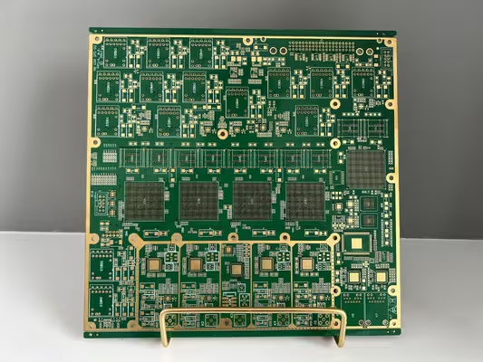
At KKPCB, advanced Megtron 7 PCB solutions are engineered for:
- AI server systems
- High-speed networking hardware
- Ultra-low-loss signal transmission
2. What Is Megtron 7 PCB?
Megtron 7 PCB is a high-performance ultra-low-loss PCB material system developed for:
- High-speed digital communication
- AI computing infrastructure
- Advanced networking applications
- High-frequency RF systems
Megtron 7 PCB materials offer:
- Extremely low dielectric loss
- Stable dielectric constant
- High thermal stability
- Excellent signal transmission performance
Compared with standard FR4 PCB materials, Megtron 7 PCB provides:
- Lower insertion loss
- Better signal integrity
- Higher transmission bandwidth capability
- Improved high-speed routing performance
This makes Megtron 7 PCB highly suitable for:
- 112G/224G high-speed systems
- AI accelerator hardware
- Data center networking equipment
- Advanced cloud computing infrastructure
3. Key Characteristics of Megtron 7 PCB
3.1 Ultra-Low Signal Loss
One of the most important advantages of Megtron 7 PCB materials is ultra-low dielectric loss.
Ultra-low-loss PCB materials help:
- Reduce insertion loss
- Minimize signal attenuation
- Improve long-distance high-speed transmission
This is critical in:
- AI server backplanes
- High-speed switch systems
- Data center networking hardware
3.2 Excellent Signal Integrity
At ultra-high data rates, signal integrity becomes highly sensitive to:
- Dielectric loss
- Surface roughness
- Crosstalk
- Reflection discontinuities
Megtron 7 PCB materials help reduce:
- Timing distortion
- Signal reflection
- High-frequency transmission degradation
These benefits improve:
- Data transmission reliability
- System stability
- High-speed communication quality
3.3 Stable Controlled Impedance Performance
Controlled impedance is essential in:
- High-speed digital PCB systems
- Differential pair routing
- AI networking hardware
Megtron 7 PCB materials provide:
- Stable dielectric performance
- Predictable impedance behavior
- Consistent signal propagation
At KKPCB, advanced stack-up optimization ensures:
- Stable impedance consistency
- Reliable ultra-high-speed transmission
- Better signal integrity performance
3.4 Excellent Thermal Reliability
High-speed AI and networking systems generate substantial heat due to:
- High processing density
- Fast switching speeds
- Increased power consumption
Megtron 7 PCB materials provide:
- Stable thermal performance
- Reliable dimensional stability
- Improved multilayer PCB reliability
These properties improve:
- Long-term operational stability
- Electrical consistency
- High-speed system reliability
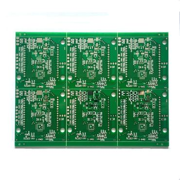
4. Applications of Megtron 7 PCB
Megtron 7 PCB technology is widely used in:
- AI servers and accelerators
- Data center networking equipment
- High-speed switch systems
- Cloud computing infrastructure
- 5G and 6G communication hardware
- High-performance computing platforms
- Ultra-high-speed storage systems
These applications require:
- Ultra-low-loss signal transmission
- Stable signal integrity
- Reliable high-speed communication capability
5. Multilayer Stack-Up Design for Megtron 7 PCB
Multilayer stack-up design is critical for:
- High-speed routing stability
- Controlled impedance consistency
- EMI suppression
- Power integrity management
Important stack-up considerations include:
- Symmetrical multilayer structures
- Dedicated reference planes
- Controlled dielectric thickness
- Differential pair isolation
Optimized stack-up design improves:
- Crosstalk reduction
- Timing accuracy
- High-speed transmission quality
6. Signal Integrity Optimization in Megtron 7 PCB
Signal integrity optimization techniques include:
- Differential pair matching
- Via stub minimization
- Ground plane continuity
- Smooth routing transitions
- Low-profile copper optimization
These methods reduce:
- Reflection loss
- Timing skew
- RF noise interference
- Transmission degradation
This is especially important in:
- 112G PAM4 systems
- AI server architectures
- High-speed data center networks
7. EMI and EMC Optimization
Ultra-high-speed PCB systems generate significant electromagnetic interference.
EMI control strategies include:
- Ground via stitching
- Controlled return current paths
- Shielding structures
- Layer isolation optimization
- Differential routing techniques
Effective EMI suppression improves:
- Signal integrity
- Communication stability
- EMC compliance performance
8. Thermal Management in Megtron 7 PCB
High-performance computing systems generate concentrated heat from:
- AI processors
- High-speed switching ICs
- Accelerator modules
- Power delivery systems
Thermal management solutions include:
- Thermal via arrays
- Copper heat-spreading layers
- Heat sink integration
- Advanced airflow structures
Efficient thermal design improves:
- System reliability
- Signal stability
- Long-term operational performance
9. Manufacturing Challenges of Megtron 7 PCB
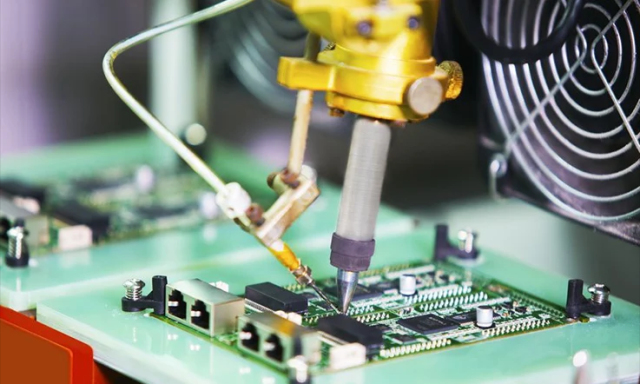
Megtron 7 PCB fabrication requires extremely high manufacturing precision.
Key manufacturing challenges include:
- Tight impedance tolerance control
- Low-profile copper processing
- Precision multilayer alignment
- Stable dielectric thickness management
- High-density routing accuracy
Ultra-high-speed PCB manufacturing must minimize:
- Surface roughness variation
- Signal discontinuities
- Transmission inconsistencies
At KKPCB, advanced PCB manufacturing technologies ensure:
- Stable electrical performance
- Reliable multilayer PCB quality
- Consistent high-speed production capability
10. Advantages of Megtron 7 PCB Compared with Standard FR4
Compared with traditional FR4 PCB materials, Megtron 7 PCB offers:
- Ultra-low dielectric loss
- Better signal integrity
- Improved high-speed transmission performance
- Higher thermal reliability
- More stable controlled impedance behavior
This makes Megtron 7 PCB ideal for:
- AI server systems
- High-speed networking hardware
- Advanced communication infrastructure
11. Future Trends in Megtron 7 PCB Technology
Future Megtron 7 PCB development focuses on:
- 224G and higher transmission systems
- AI supercomputing infrastructure
- Ultra-high-density networking hardware
- Advanced cloud computing architectures
- Next-generation communication systems
Emerging technologies require:
- Faster data transmission
- Lower insertion loss
- Better signal integrity precision
- More advanced multilayer PCB integration
12. Conclusion
Megtron 7 PCB technology is a critical solution for advanced:
- AI computing systems
- Ultra-high-speed networking hardware
- Data center infrastructure
- High-frequency communication electronics
Through optimized:
- Ultra-low-loss PCB materials
- Controlled impedance routing
- Signal integrity engineering
- Multilayer stack-up design
- Advanced manufacturing precision
engineers can achieve:
- Faster data transmission
- Better communication stability
- Reduced signal attenuation
- Higher system reliability
With extensive expertise in ultra-high-speed PCB engineering and multilayer manufacturing, KKPCB delivers advanced PCB solutions for next-generation AI and networking systems.
