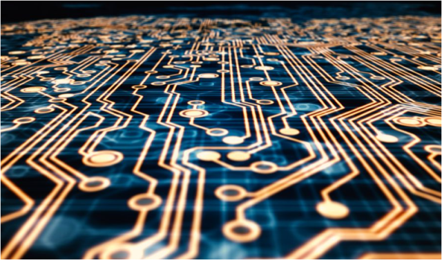
Why High Speed PCB Technology Is Critical
Modern electronic systems are rapidly evolving toward:
- Faster data transmission
- Higher processing bandwidth
- AI-driven computing platforms
- High-speed networking infrastructure
- Real-time communication systems
Applications such as:
- AI servers
- Data centers
- 5G communication equipment
- High-performance computing systems
- Cloud networking infrastructure
all rely heavily on advanced High Speed PCB technology.
As operating speeds continue increasing, PCB design becomes more sensitive to:
- Signal reflection
- Crosstalk interference
- Electromagnetic noise
- Power instability
- Transmission loss
Traditional PCB design methods often struggle to support:
- Multi-gigabit signal transmission
- High-frequency communication
- Dense high-speed routing architectures
As a result, advanced High Speed PCB solutions are essential for:
- Stable high-speed communication
- Reliable signal integrity
- Efficient power distribution
At KKPCB, advanced high-speed PCB solutions are engineered for:
- AI computing systems
- High-bandwidth networking platforms
- High-frequency communication electronics
What Is a High Speed PCB?
A High Speed PCB is a printed circuit board specifically designed for:
- High-frequency signal transmission
- Multi-gigabit data communication
- High-bandwidth networking systems
- Advanced digital processing platforms
High Speed PCB systems are commonly used in:
- AI servers
- Data center switches
- High-performance computing platforms
- 5G communication systems
- Networking routers and switches
- Aerospace communication electronics
These PCB systems must provide:
- Excellent signal integrity
- Stable power integrity
- Controlled impedance consistency
- Low transmission loss
- Reliable thermal performance
Key Characteristics of High Speed PCB
Excellent Signal Integrity
Signal integrity is one of the most critical factors in High Speed PCB design.
High-speed signals are highly sensitive to:
- Reflection noise
- Crosstalk interference
- Timing mismatch
- Electromagnetic coupling
- Transmission discontinuities
High Speed PCB design focuses on:
- Differential pair routing
- Return path optimization
- Layer isolation techniques
- Controlled routing structures
These methods improve:
- Data transmission accuracy
- Communication stability
- System reliability
Controlled Impedance Routing
Controlled impedance is essential for:
- High-speed digital interfaces
- PCIe communication
- DDR memory routing
- Ethernet networking systems
- High-frequency communication channels
High Speed PCB routing must carefully optimize:
- Trace geometry
- Layer stack-up structures
- Dielectric thickness
- Signal return paths
Stable impedance control improves:
- Signal consistency
- Timing accuracy
- Transmission quality
At KKPCB, advanced stack-up optimization ensures:
- Reliable multi-gigabit transmission
- Stable high-frequency communication
- Accurate impedance consistency
Low-Loss PCB Materials
As data rates increase, PCB materials significantly affect:
- Signal attenuation
- Transmission stability
- High-frequency performance
High Speed PCB applications commonly use:
- Low-loss PCB laminates
- High-speed dielectric materials
- Advanced multilayer substrates
These materials improve:
- Signal transmission quality
- Communication distance
- High-speed reliability
Low-loss PCB materials are especially important for:
- AI server systems
- Data center networking
- 5G communication platforms
Power Integrity Optimization
High-speed systems require stable power delivery for:
- AI processors
- High-speed CPUs
- Memory systems
- Networking ASICs
Power integrity optimization techniques include:
- Power plane balancing
- Decoupling capacitor optimization
- Low-noise power routing
- Ground plane continuity
These methods improve:
- System stability
- Signal consistency
- High-speed operational reliability
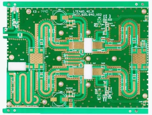
PCB Materials for High Speed PCB
Material selection strongly affects:
- Signal integrity
- Insertion loss
- Thermal performance
- Mechanical reliability
Common High Speed PCB materials include:
Important material properties include:
- Low dielectric loss
- Stable dielectric constant
- Excellent thermal stability
- High-frequency consistency
Multilayer Stack-Up Design for High Speed PCB
Modern high-speed systems commonly use:
- Multilayer PCB architectures
- Dedicated power and ground planes
- Differential routing layers
- Signal isolation structures
Proper multilayer stack-up improves:
- Signal integrity
- EMI suppression
- Power integrity
- Routing efficiency
Optimized PCB structures reduce:
- Crosstalk interference
- Power noise
- Transmission instability
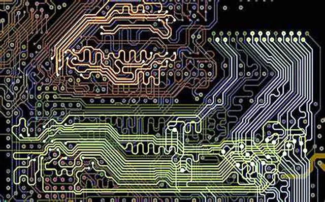
High-Speed Routing Optimization
Proper routing design is critical for maintaining:
- Signal timing consistency
- Differential pair balance
- Stable transmission quality
High-speed routing techniques include:
- Differential pair matching
- Length tuning optimization
- Via stub reduction
- Smooth routing transitions
- Return path continuity
These methods improve:
- Data transmission reliability
- Timing stability
- Multi-gigabit signal performance
EMI and EMC Optimization
High-speed electronic systems generate significant electromagnetic interference.
EMI suppression strategies include:
- Ground shielding structures
- Via stitching optimization
- Layer separation management
- Differential signal routing
- Controlled return current paths
Effective EMI control improves:
- Communication reliability
- Signal quality
- EMC compliance performance
Thermal Management in High Speed PCB
High-performance systems generate concentrated heat from:
- AI processors
- CPUs and GPUs
- Networking ASICs
- High-speed communication modules
Thermal management solutions include:
- Thermal via arrays
- Copper heat-spreading structures
- Heat sink integration
- Thermal balancing stack-up design
Efficient thermal management improves:
- System reliability
- Processing stability
- Long-term operational lifespan
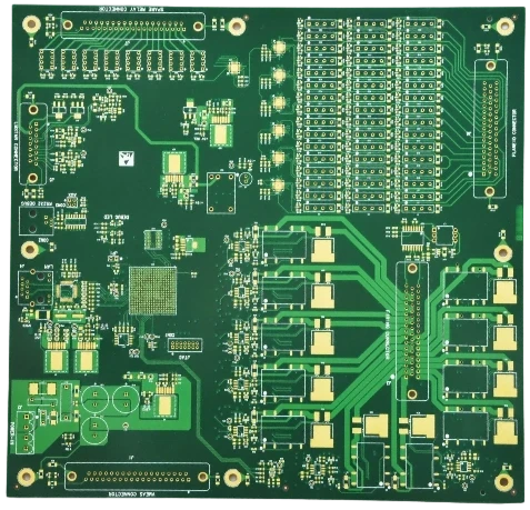
Manufacturing Challenges of High Speed PCB
High Speed PCB fabrication requires advanced manufacturing precision.
Key manufacturing challenges include:
- Tight impedance tolerance control
- Fine-line routing accuracy
- Stable multilayer alignment
- Low-loss material processing
- Signal integrity consistency
High-speed PCB manufacturing must minimize:
- Transmission discontinuities
- Surface roughness variation
- Timing instability
At KKPCB, advanced manufacturing technologies ensure:
- Stable high-speed transmission performance
- Reliable multilayer PCB quality
- Consistent high-frequency production capability
Applications of High Speed PCB
High Speed PCB technology is widely used in:
- AI server systems
- Data center networking
- High-performance computing platforms
- 5G communication infrastructure
- Cloud networking equipment
- Aerospace communication systems
- High-speed industrial electronics
These applications require:
- Multi-gigabit signal transmission
- Stable communication performance
- Reliable signal integrity
Future Trends in High Speed PCB Technology
Future High Speed PCB development focuses on:
- AI-driven computing platforms
- 800G and beyond networking systems
- Ultra-high-speed communication infrastructure
- Advanced low-loss PCB materials
- Compact high-density multilayer architectures
Emerging technologies require:
- Faster data transmission
- Lower signal loss
- Better thermal efficiency
- Higher routing density
Conclusion
High Speed PCB technology is essential for modern:
- AI computing systems
- High-bandwidth networking infrastructure
- High-frequency communication platforms
Through optimized:
- Controlled impedance routing
- Signal integrity engineering
- Power integrity management
- Multilayer stack-up design
- Advanced manufacturing precision
engineers can achieve:
- Faster data transmission
- Better communication reliability
- Reduced signal loss
- Higher system performance
With extensive expertise in high-speed PCB engineering and advanced multilayer manufacturing, KKPCB delivers advanced PCB solutions for next-generation computing and communication technologies.
