PCB manufacturing - KKPCB
 
HomeTag

PCB manufacturing - KKPCB

Effective Strategies for PCB Panelization

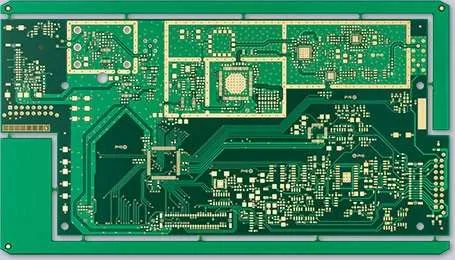
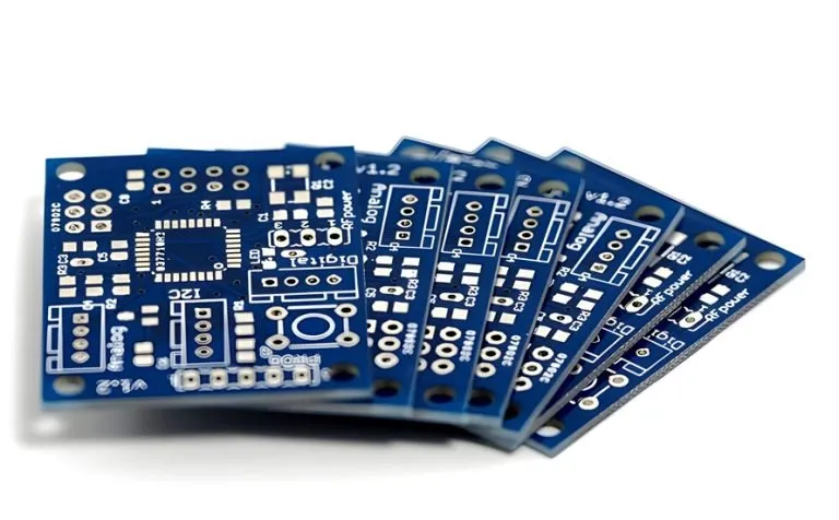
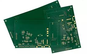
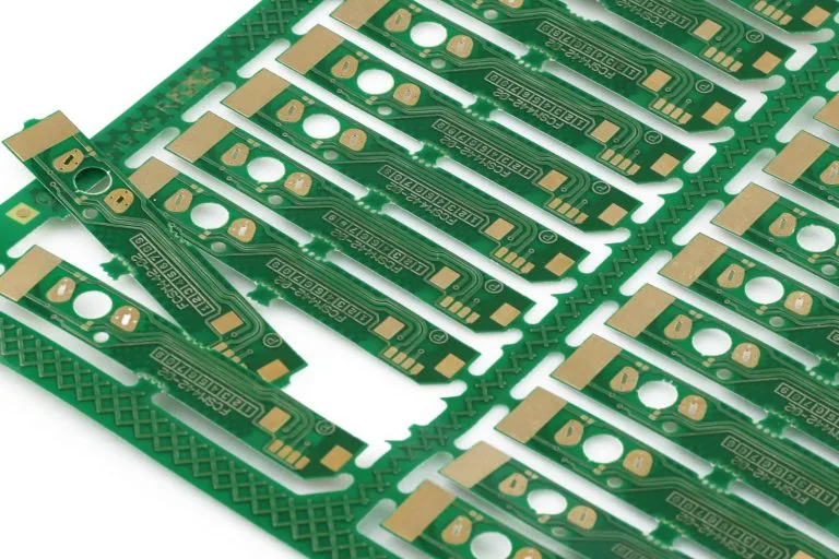
Handling small circuit boards during automated assembly can lead to defects and inefficiencies. To overcome this challenge, PCB panelization—the process of creating PCB panels from smaller boards—plays a vital role. This technique not only ensures improved handling during assembly but also reduces costs and minimizes defects. Here’s a comprehensive guide to panelizing PCBs, including methods, techniques,...

Multilayer PCB Manufacturing Process: A Complete Step-by-Step Guide

Multilayer PCBs (Printed Circuit Boards) are the heart of complex modern electronics, consisting of three or more conductive copper layers separated by insulating dielectric materials. Unlike simpler boards, they offer higher circuit density and improved signal integrity, making them essential for everything from smartphones to aerospace technology. Step 1: Design and Data Preparation The process...

Advantages and applications of single-sided PCB

The Single-Sided PCB (Single-Layer PCB) is the most fundamental and widely used type of circuit board in the electronics industry. Featuring a single layer of conductive copper laminated onto a rigid base material (typically FR-4 or CEM-1), these boards are the backbone of high-volume, cost-sensitive electronics. For PCB manufacturing partners like KKPCB, the single-sided board remains a staple for projects...

Solder Paste and Stencil Considerations for Double-Sided PCBs

The Challenge of Double-Sided PCB Assembly In modern SMT PCB assembly, double-sided PCBs are widely used to increase component density and optimize space utilization. However, assembling components on both sides of a printed circuit board introduces additional complexity in solder paste printing and stencil design. Proper control of solder paste and stencil parameters is critical...

Understanding and Improving PCB Open Circuits: Causes and Solutions

Why PCB Open Circuits Matter In PCB manufacturing and PCB assembly, PCB open circuits are one of the most common and critical defects affecting electrical performance and product reliability. An open circuit occurs when an electrical path is unintentionally broken, preventing current from flowing through the circuit. For industries requiring high reliability—such as automotive electronics,...

Common Problems and Solutions for Substrates in PCB Design

In modern PCB design, the choice and handling of substrate materials play a critical role in determining the overall performance, reliability, and manufacturability of the circuit board. Substrate-related issues can lead to serious defects such as poor solderability, delamination, signal loss, and even complete product failure. This article outlines the most common substrate problems encountered...

Industrial PCB Production

Industrial PCB Production In today’s rapidly evolving industrial landscape, Printed Circuit Boards (PCBs) serve as the critical backbone of automation systems, control equipment, heavy machinery, robotics, and smart manufacturing solutions. Industrial PCB production demands far higher standards than consumer electronics. Boards must deliver exceptional reliability, durability under extreme conditions (vibration, temperature fluctuations, humidity, and dust),...

Effective Strategies for PCB Panelization

In modern PCB manufacturing, PCB panelization is a crucial process that improves production efficiency, reduces cost, and enhances assembly accuracy. Whether for multilayer PCBs, rigid circuit boards, or PCBA assembly, optimizing PCB panel design can significantly impact yield and overall product quality. What Is PCB Panelization? PCB panelization is the process of combining multiple individual...

Advanced PCB Footprint Generator: Key to Efficient PCB Design

1. Introduction: Why PCB Footprint Accuracy Matters in Modern Electronics In modern PCB design and electronic product development, accuracy at the earliest design stage directly determines manufacturing success, cost efficiency, and product reliability. One of the most critical elements in PCB layout design is the PCB footprint, which defines the physical land pattern for electronic...