In modern PCB manufacturing, PCB panelization is a crucial process that improves production efficiency, reduces cost, and enhances assembly accuracy. Whether for multilayer PCBs, rigid circuit boards, or PCBA assembly, optimizing PCB panel design can significantly impact yield and overall product quality.
What Is PCB Panelization?
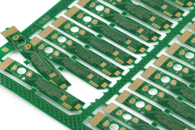
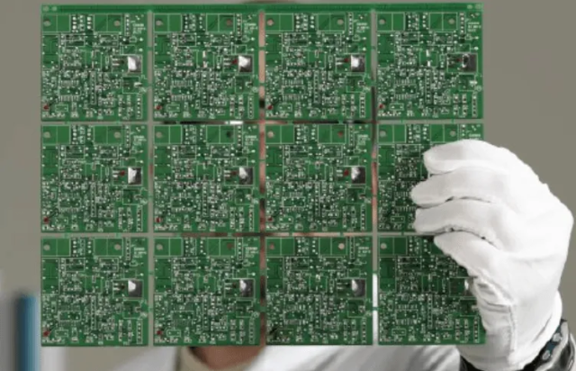
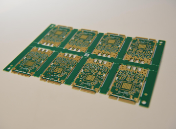
PCB panelization is the process of combining multiple individual printed circuit boards (PCBs) into a single panel for manufacturing and assembly. This allows for efficient handling during SMT assembly, wave soldering, and automated production processes.
Common PCB panelization methods include:
- V-score (V-cut) panelization
- Tab routing with breakaway tabs
- Solid panelization with rails
Key Benefits of PCB Panelization
1. Improved Manufacturing Efficiency
By grouping multiple boards into one panel, PCB fabrication and PCBA assembly processes become faster and more cost-effective.
2. Reduced Production Costs
PCB panelization design minimizes material waste and optimizes machine usage, lowering overall production costs.
3. Enhanced Assembly Accuracy
Panels provide better stability during SMT placement, improving component alignment and reducing errors.
4. Better Handling and Protection
Small or irregular-shaped PCBs are easier to handle when panelized, reducing the risk of damage during manufacturing.
Effective PCB Panelization Strategies
1. Optimize Panel Size
Choosing the right PCB panel size is essential. It should match the manufacturing equipment capabilities while maximizing board count per panel.
Best practice:
- Align panel dimensions with standard fabrication sizes
- Avoid excessive unused space
2. Choose the Right Panelization Method
Selecting the appropriate PCB panelization technique depends on board design:
- V-score panelization: Ideal for rectangular rigid PCBs
- Tab routing: Suitable for complex shapes
- Combination methods: For mixed designs
3. Design Proper Breakaway Tabs
In tab routing panelization, breakaway tabs should be carefully designed:
- Use mouse bites (perforations) for easy separation
- Ensure sufficient tab strength during assembly
- Avoid placing tabs near sensitive components
4. Maintain Adequate Spacing
Proper spacing between boards in a panel is critical for:
- Preventing short circuits
- Allowing clean separation
- Ensuring accurate routing
5. Add Tooling Rails and Fiducials
PCB panel design should include:
- Tooling rails for conveyor handling
- Fiducial marks for precise SMT alignment
These features improve automation efficiency in PCBA manufacturing.
6. Consider Component Placement
Avoid placing components too close to board edges or breakaway tabs to prevent damage during depanelization.
7. Ensure Structural Stability
Panels must remain rigid during processing. Adding support structures or rails improves stability for thin or flexible boards.
Common Mistakes in PCB Panelization
- Incorrect panel size selection
- Poor tab placement causing board damage
- Insufficient spacing between PCBs
- Missing fiducials for SMT alignment
- Ignoring assembly process requirements
Avoiding these mistakes ensures a higher yield in PCB production.
Why Choose KKPCB for PCB Panelization and Manufacturing?
1. Expertise in PCB Panel Design
KKPCB provides professional PCB panelization solutions tailored to your product design and assembly needs.
2. Advanced Manufacturing Capabilities
With modern equipment, KKPCB ensures high-precision PCB fabrication and efficient panel processing.
3. End-to-End PCBA Services
From PCB design to SMT assembly, KKPCB offers complete solutions, including optimized panelization strategies.
4. Quality and Cost Optimization
KKPCB helps reduce costs while maintaining high quality through optimized PCB panel layouts.
Applications of PCB Panelization
PCB panelization is widely used in:
- Consumer electronics
- Industrial control systems
- Automotive electronics
- Communication devices
Conclusion
Effective PCB panelization strategies are essential for improving manufacturing efficiency, reducing costs, and ensuring product quality. By optimizing panel size, layout, spacing, and depanelization methods, manufacturers can achieve higher yields and better performance.
Partnering with KKPCB ensures expert support in PCB panel design and PCBA manufacturing, helping you maximize efficiency and reliability.
