HomeTag

PCB Design - KKPCB

Relationship Between Current and Line Width in PCB Design

In PCB design, trace width is one of the fundamental parameters that directly affects the electrical performance, thermal reliability, and manufacturing quality of a circuit board. When current flows through a PCB trace, the conductor generates heat due to electrical resistance. If the trace width is insufficient, excessive temperature rise may cause: Copper trace overheating...
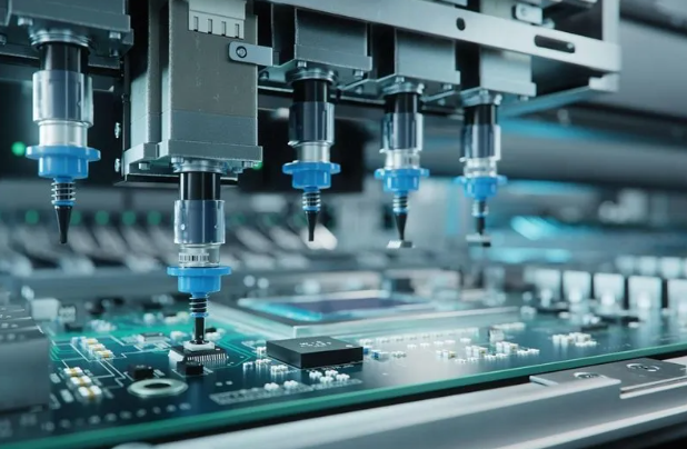
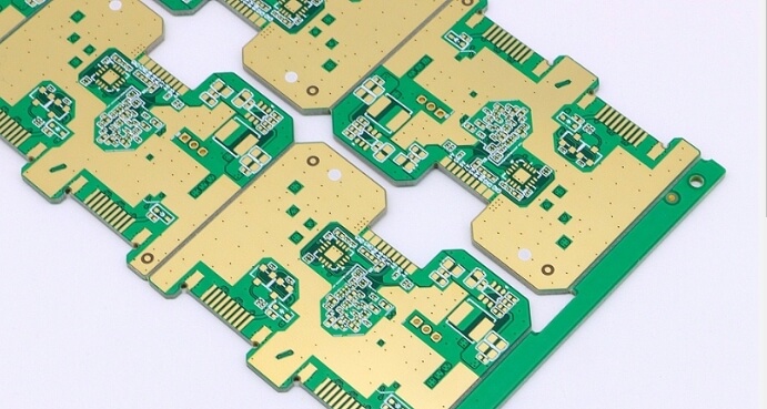
PCB for SMT (Surface Mount Technology): Choosing the Right PCB for SMD Components

With the rapid development of electronic products toward miniaturization, higher integration, and automated manufacturing, Surface Mount Technology (SMT) has become one of the most widely used PCB assembly methods in modern electronics. Unlike traditional through-hole components, Surface Mount Devices (SMD components) are mounted directly onto the surface of a PCB, allowing manufacturers to achieve: Higher...

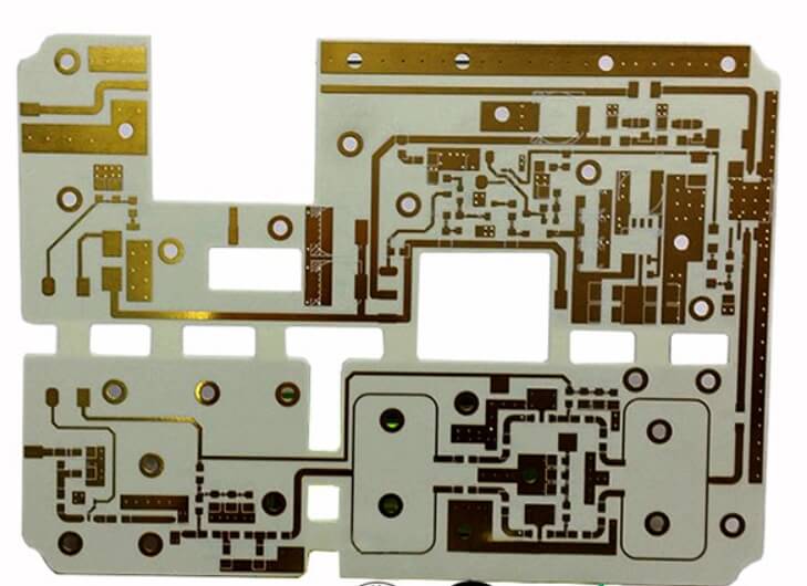
What are the high-frequency PCB boards? How to choose?

When processing and testing high-frequency PCB boards and high-frequency antennas, beginners often choose incorrect high-frequency PCBs, resulting in unsatisfactory product results. Let’s talk briefly today, what are the PCB high-frequency boards? How to choose? Definition of PCB high-frequency boards High-frequency circuit boards refer to special PCB circuit boards with higher electromagnetic frequencies. They are used in high-frequency (frequency greater...

Grounding method in multilayer PCB circuit board

In modern multilayer PCB circuit board design, selecting the correct grounding method is essential for ensuring optimal signal integrity, minimizing electromagnetic interference (EMI), and maintaining stable power integrity. A well-designed grounding system not only improves overall PCB performance but also enhances the reliability of high-speed and high-frequency electronic applications. One of the most widely used...

About PCB Layer Stackup

A PCB Layer Stackup refers to the arrangement of conductive copper layers and insulating dielectric materials that make up a multilayer PCB. In the era of high-speed digital electronics and 5G, the stackup is no longer just a mechanical carrier; it is a critical tool for managing signal integrity, power distribution, and electromagnetic compatibility (EMC). A well-engineered stackup from KKPCB ensures...

Basic Knowledge You Need to Master for PCB Design

PCB (Printed Circuit Board) design is a fundamental process in electronic product development. A well-designed PCB not only provides electrical connections between components but also directly affects: Signal integrity Power stability Electromagnetic compatibility (EMC) Thermal performance Manufacturing reliability With the increasing complexity of modern electronic systems, PCB design is no longer limited to simple component...

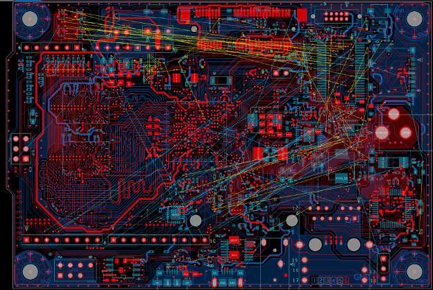
Basic Principles and Operations of PCB Wiring

PCB wiring, also known as PCB routing, is one of the most critical stages in printed circuit board design. It determines how electrical signals and power are transmitted between components and directly affects the performance, reliability, and manufacturability of electronic products. With modern electronic systems moving toward higher speed, higher density, and greater integration, PCB...

Blind Via and Buried Via

In modern PCB design, Blind Via and Buried Via technologies play a critical role in achieving high-density interconnect (HDI) structures, improving signal integrity, and optimizing PCB layout performance. As electronic devices continue to evolve toward miniaturization, high speed, and high functionality, the use of blind vias and buried vias has become increasingly essential in advanced...

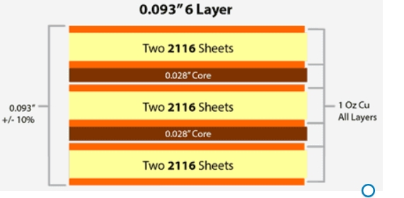
6 layer PCB Stackup,Thickness and Manufacturing

Printed circuit boards (PCBs) have evolved from simple single or double layer boards to complex multilayer boards with 6 or more layers to accommodate increasing component density and interconnectivity needs. 6 layer PCBs provide more flexibility for routing, plane separation and enable partitioning of circuits across layers. However, designing the 6 layer stackup requires careful planning to utilize...