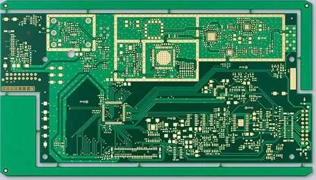
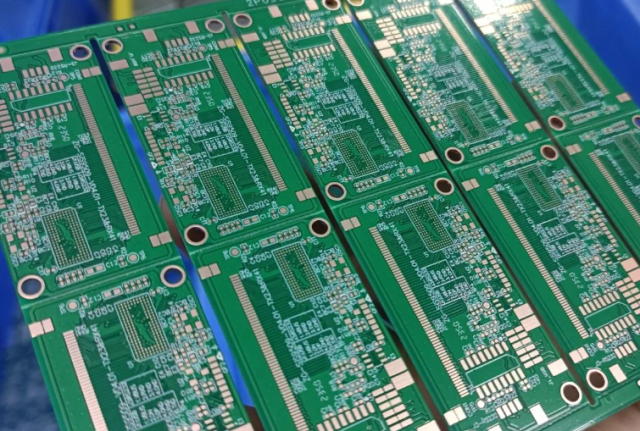
In modern multilayer PCB circuit board design, selecting the correct grounding method is essential for ensuring optimal signal integrity, minimizing electromagnetic interference (EMI), and maintaining stable power integrity. A well-designed grounding system not only improves overall PCB performance but also enhances the reliability of high-speed and high-frequency electronic applications.
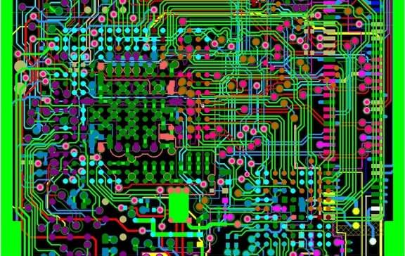
One of the most widely used grounding methods in multilayer PCB circuit boards is the implementation of a solid ground plane. A continuous ground plane provides a low-impedance return path for signals, significantly reducing noise, crosstalk, and EMI issues. In high-speed PCB design, a dedicated ground layer adjacent to signal layers is critical for maintaining controlled impedance and reducing signal reflection.
Another important grounding method is single-point grounding, which is commonly used in analog circuit design. In this approach, all ground connections converge at a single reference point, effectively preventing ground loops and minimizing noise coupling. This method is particularly suitable for low-frequency PCB applications where precision and noise isolation are crucial.
For more complex multilayer PCB circuit boards, multi-point grounding is often applied, especially in high-frequency PCB designs. By connecting ground points at multiple locations, this grounding method reduces ground impedance and enhances signal return paths, making it ideal for RF circuits, communication systems, and high-speed digital circuits.
A hybrid grounding method that combines single-point grounding and multi-point grounding is frequently used in mixed-signal multilayer PCB designs. This approach separates analog ground (AGND) and digital ground (DGND) while maintaining a controlled connection point to reduce noise interference between analog and digital sections. Proper ground partitioning is essential for improving signal integrity and preventing EMI problems.
In addition to grounding strategies, the use of via stitching and ground vias plays a crucial role in enhancing the effectiveness of the grounding method in multilayer PCB circuit boards. By placing multiple ground vias around high-speed traces and critical components, designers can reduce loop area, improve shielding performance, and further suppress EMI.
When designing the grounding method for multilayer PCB circuit boards, engineers must consider factors such as layer stack-up design, component placement, signal routing, and thermal management. A properly optimized grounding structure can significantly improve PCB signal quality, reduce electromagnetic emissions, and ensure compliance with EMC standards.
In conclusion, choosing the right grounding method in multilayer PCB circuit board design is fundamental to achieving high-performance PCB systems. Whether using ground planes, single-point grounding, multi-point grounding, or hybrid approaches, effective grounding design directly impacts signal integrity, EMI control, and overall PCB reliability in advanced electronic applications.
