HomeTag

multilayer PCB - KKPCB

Advanced PCBs – Design, Manufacturing, and Assembly

Advanced PCBs represent the cutting edge of printed circuit board technology, enabling compact, high-performance, and highly reliable electronic systems for demanding applications such as 5G/6G infrastructure, ADAS automotive radar, AI computing, aerospace electronics, Industrial IoT, and medical devices. These boards go far beyond standard FR-4 designs, incorporating HDI (High-Density Interconnect), rigid-flex, high-frequency low-loss materials, heavy...
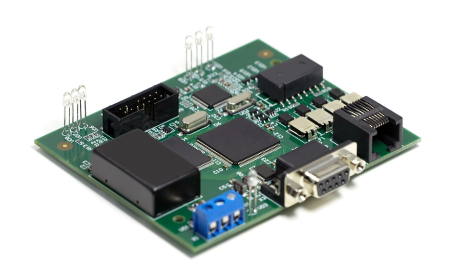
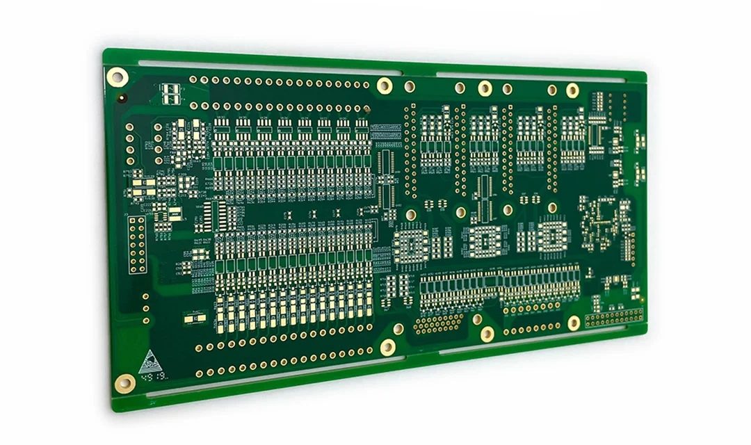
Printed Circuit Board Basics: From Design to Final Artwork

Understanding the Foundation of PCB Technology   A Printed Circuit Board (PCB) is the foundation of nearly every modern electronic product. From: consumer electronics industrial automation systems automotive electronics medical devices aerospace communication equipment high-speed networking hardware PCBs provide the essential platform for: electrical connectivity signal transmission component mounting power distribution As electronic products continue...

Multilayer PCB Manufacturing Process: A Complete Step-by-Step Guide

With the increasing demand for higher circuit density, faster signal transmission, and more complex electronic functions, multilayer printed circuit boards (PCBs) have become a fundamental technology in modern electronic products. Unlike single-layer or double-sided PCBs, multilayer PCBs integrate multiple copper layers and insulating dielectric materials into one compact structure, allowing engineers to achieve complex routing,...

Grounding method in multilayer PCB circuit board

In modern multilayer PCB circuit board design, selecting the correct grounding method is essential for ensuring optimal signal integrity, minimizing electromagnetic interference (EMI), and maintaining stable power integrity. A well-designed grounding system not only improves overall PCB performance but also enhances the reliability of high-speed and high-frequency electronic applications. One of the most widely used...

About PCB Layer Stackup

A PCB Layer Stackup refers to the arrangement of conductive copper layers and insulating dielectric materials that make up a multilayer PCB. In the era of high-speed digital electronics and 5G, the stackup is no longer just a mechanical carrier; it is a critical tool for managing signal integrity, power distribution, and electromagnetic compatibility (EMC). A well-engineered stackup from KKPCB ensures...

N4800-20 High-Speed Multifunctional Epoxy Laminate & Prepreg

As the demand for high-bandwidth data transmission and 5G infrastructure grows, the choice of PCB base materials becomes a critical factor in system performance. N4800-20, developed by Nelco, is a high-speed, multifunctional epoxy laminate and prepreg system designed specifically for the next generation of high-speed digital (HSD) applications. It offers a unique balance of thermal reliability and superior signal integrity, making...

Experience Sharing in Multi-Layer PCB Impedance Line Routing

With the continuous development of high-speed electronic systems, PCB design is facing increasingly demanding requirements for signal transmission performance. In applications such as communication equipment, industrial control systems, automotive electronics, semiconductor testing equipment, and RF systems, maintaining stable signal quality has become a key factor affecting product reliability. In multilayer PCB design, impedance-controlled routing is...

The Multilayer PCB: What it is, how it works, and when you should use it

In the world of electronics, where technological advancements occur rapidly, the multilayer PCB has established its dominance. Over the past few decades, multilayer printed circuit boards have become an indispensable part of modern electronic devices, enabling them to meet the complex needs of today’s consumers. From Single to Double-sided PCB to Multilayer PCB Traditionally, printed circuit boards...

Multilayer PCBs: Overview, Manufacturing, and Design Considerations

With the continuous evolution of electronic products toward higher functionality, smaller form factors, and increased signal complexity, traditional single-layer and double-layer PCBs are often unable to meet modern design requirements. Multilayer PCBs have become an essential technology for advanced electronic systems by providing more routing space, improved electrical performance, and enhanced design flexibility. By integrating...

Blind Via and Buried Via

In modern PCB design, Blind Via and Buried Via technologies play a critical role in achieving high-density interconnect (HDI) structures, improving signal integrity, and optimizing PCB layout performance. As electronic devices continue to evolve toward miniaturization, high speed, and high functionality, the use of blind vias and buried vias has become increasingly essential in advanced...