Understanding the Foundation of PCB Technology
A Printed Circuit Board (PCB) is the foundation of nearly every modern electronic product. From:
- consumer electronics
- industrial automation systems
- automotive electronics
- medical devices
- aerospace communication equipment
- high-speed networking hardware
PCBs provide the essential platform for:
- electrical connectivity
- signal transmission
- component mounting
- power distribution
As electronic products continue evolving toward:
- higher speed
- smaller size
- greater functionality
- higher reliability
understanding the complete PCB design and manufacturing process becomes increasingly important.
This article explores the fundamentals of Printed Circuit Board basics, covering:
- PCB design principles
- PCB layout engineering
- PCB materials
- circuit routing
- PCB fabrication
- PCB artwork generation
- manufacturing preparation
from the initial concept all the way to the final PCB artwork stage.
What Is a Printed Circuit Board (PCB)?
A Printed Circuit Board (PCB) is a flat insulating board containing:
- conductive copper traces
- electronic interconnections
- component mounting pads
- plated holes and vias
The PCB mechanically supports and electrically connects electronic components through:
- copper circuitry
- solder joints
- conductive pathways
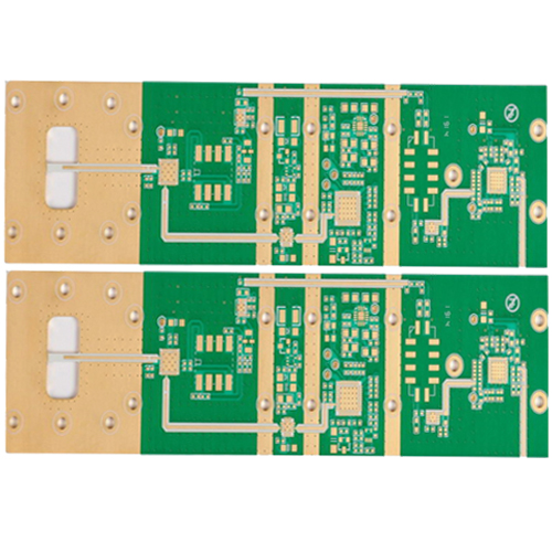
Modern PCB technologies include:
- single-sided PCB
- double-sided PCB
- multilayer PCB
- HDI PCB
- flexible PCB
- rigid-flex PCB
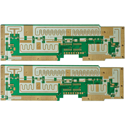
- RF and microwave PCB
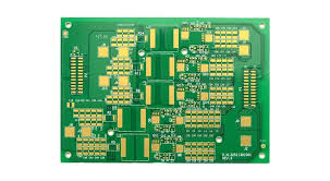
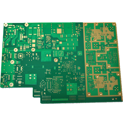
Basic PCB Structure
A standard PCB structure includes:
- PCB substrate material
- copper conductive layers
- solder mask coating
- silkscreen printing
- surface finish
Additional structures may include:
- plated through holes (PTH)
- blind vias
- buried vias
- controlled impedance layers
Main PCB Materials
1. FR4 PCB Material
The most widely used PCB substrate.
Advantages:
- good insulation properties
- strong mechanical stability
- low manufacturing cost
Applications:
- consumer electronics
- industrial PCB systems
- power supply PCB products
2. High-Frequency PCB Materials
Used for:
- RF PCB
- microwave PCB
- mmWave PCB applications
Characteristics:
- low dielectric loss
- stable dielectric constant
- excellent signal integrity
3. Flexible PCB Materials
Flexible substrates allow:
- bending capability
- compact electronic packaging
- lightweight PCB structures
4. Metal Core PCB Materials
Used in:
- LED PCB
- power electronics
- thermal management systems
Advantages:
- excellent heat dissipation
- improved thermal conductivity
PCB Design Basics
1. Schematic Design
PCB development begins with:
- electronic circuit schematic creation
The schematic defines:
- component connectivity
- signal flow
- electrical functionality
Design software commonly includes:
- Altium Designer
- KiCad
- Cadence
- Mentor Graphics
2. PCB Layout Design
After schematic completion, engineers create the:
- PCB layout
- component placement
- routing structure
PCB layout design directly affects:
- signal integrity
- manufacturability
- thermal performance
- EMI behavior
3. Component Placement
Proper component placement improves:
- signal routing efficiency
- thermal management
- assembly reliability
Important considerations:
- signal flow direction
- high-speed signal isolation
- power distribution
- heat generation areas
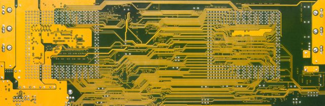
4. PCB Routing
PCB routing creates electrical connections between components.
Routing types include:
- signal routing
- power routing
- ground routing
- differential pair routing
High-speed PCB routing requires:
- controlled impedance
- length matching
- crosstalk reduction
- signal integrity optimization
5. Ground Plane and Power Plane Design
Ground and power planes improve:
- signal stability
- EMI suppression
- return current management
- power distribution efficiency
Multilayer PCB structures commonly include:
- dedicated ground layers
- power distribution layers
PCB Design Rules and Constraints
1. Trace Width and Spacing
Trace width affects:
- current carrying capacity
- thermal performance
- impedance control
Spacing impacts:
- electrical isolation
- manufacturability
- signal integrity
2. Via Design
Vias provide interconnection between PCB layers.
Common via types:
- through-hole vias
- blind vias
- buried vias
- microvias
Proper via design improves:
- routing density
- signal transmission
- PCB reliability
3. Controlled Impedance PCB Design
High-speed PCB and RF PCB applications require:
- precise impedance control
Important for:
- signal integrity
- high-frequency performance
- differential pair routing
4. Thermal Management Design
Thermal optimization methods:
- thermal vias
- copper balancing
- heat sinks
- metal core PCB structures
Proper thermal management improves:
- long-term PCB reliability
- component lifespan
PCB Artwork Generation
1. What Is PCB Artwork?
PCB artwork refers to the final graphical manufacturing data used for:
- PCB fabrication
- copper etching
- drilling
- solder mask generation
- silkscreen printing
The artwork precisely defines:
- copper traces
- pads
- vias
- board outline
- assembly markings
2. Gerber File Generation
The most common PCB artwork format is:
- Gerber data
Gerber files contain:
- copper layer information
- solder mask layers
- silkscreen artwork
- drill data
These files are used directly by:
- PCB fabrication factories
- CAM engineering systems
3. Drill File Generation
Drill files define:
- hole locations
- via sizes
- plated and non-plated holes
Accurate drill data is essential for:
- multilayer PCB alignment
- assembly precision
4. PCB Stack-Up Documentation
Stack-up files define:
- layer arrangement
- dielectric thickness
- copper thickness
- impedance structures
Critical for:
- controlled impedance PCB manufacturing
- multilayer PCB fabrication
PCB Design Verification and DFM
1. Design Rule Check (DRC)
DRC verifies:
- trace spacing
- clearance rules
- via dimensions
- manufacturing compatibility
2. Electrical Rule Check (ERC)
ERC identifies:
- connection errors
- signal conflicts
- schematic inconsistencies
3. Design for Manufacturability (DFM)
DFM analysis improves:
- PCB production yield
- assembly reliability
- manufacturing efficiency
PCB Fabrication Basics
1. PCB Material Preparation
Selection of:
- substrate material
- copper thickness
- laminate structure
2. Imaging and Etching
Copper patterns are transferred and etched onto the PCB surface.
3. Drilling and Via Formation
Mechanical or laser drilling creates:
- holes
- vias
- interconnections
4. Solder Mask and Silkscreen
Protective coatings and component markings are applied.
5. Surface Finish Processing
Common finishes:
- HASL
- ENIG
- immersion silver
- OSP
6. Electrical Testing and Inspection
Includes:
- AOI inspection
- flying probe testing
- continuity verification
Applications of PCB Technology
PCB technology is widely used in:
- consumer electronics
- automotive electronics
- industrial automation
- aerospace systems
- telecommunications
- medical electronics
- AI computing hardware
Future Trends in PCB Design and Manufacturing
1. HDI PCB Technology
Increasing routing density and miniaturization.
2. High-Speed PCB Design
Supporting:
- AI systems
- data centers
- high-speed communication
3. RF and mmWave PCB Development
Enabling:
- 5G and 6G communication
- automotive radar
- satellite systems
4. Advanced PCB Materials
Development of:
- ultra-low-loss laminates
- high thermal conductivity materials
- flexible hybrid substrates
Conclusion
Understanding Printed Circuit Board basics from design to final artwork is essential for successful electronic product development.
A complete PCB workflow includes:
- schematic design
- PCB layout engineering
- routing optimization
- impedance control
- thermal management
- Gerber artwork generation
- PCB fabrication preparation
As modern electronics continue advancing toward:
- higher speed
- smaller size
- greater integration
- improved reliability
advanced PCB design and fabrication technology will continue playing a critical role in enabling next-generation electronic systems.
