multilayer PCB - KKPCB
 
HomeTag

multilayer PCB - KKPCB

Impedance Controlled PCB: Advanced PCB Design for Stable High-Speed and RF Signal Transmission

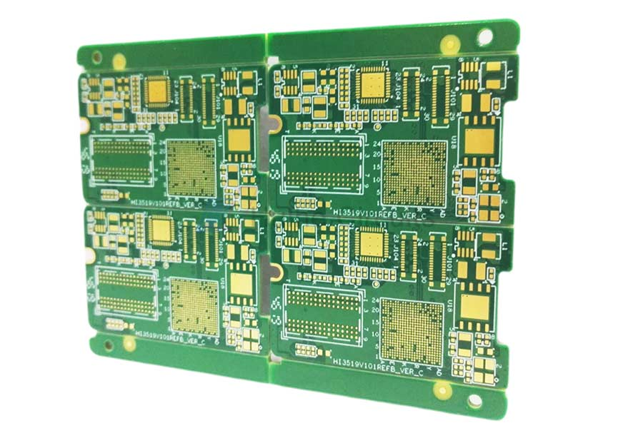
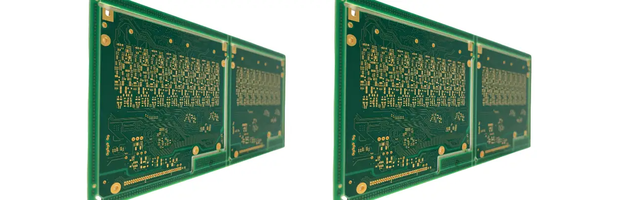
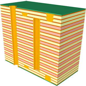
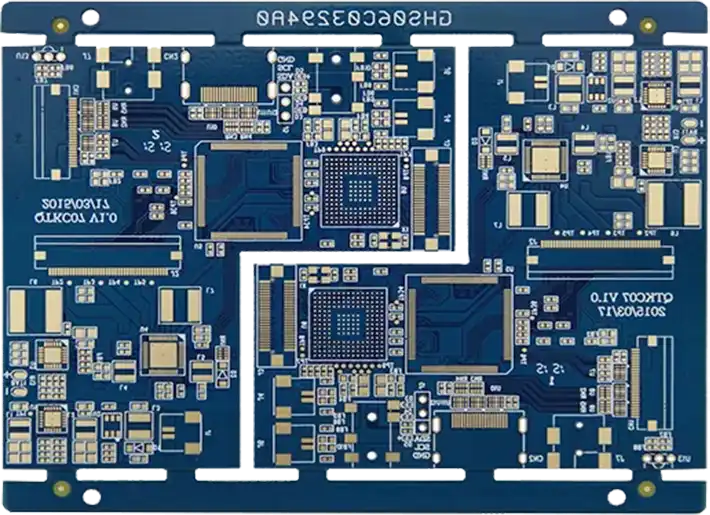
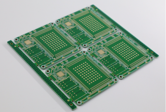
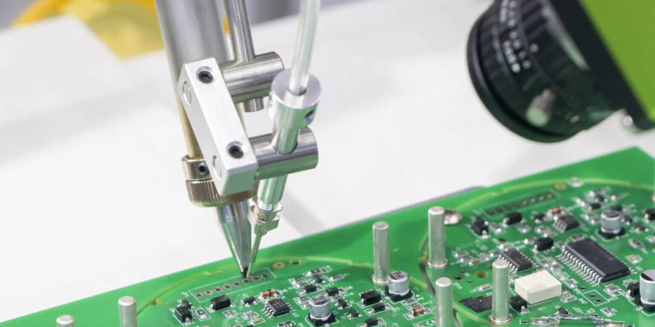
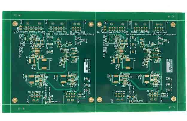
1.Why Impedance Controlled PCB Technology Is Essential As modern electronic systems continue evolving toward: Higher operating frequencies Faster data transmission Greater bandwidth requirements More compact electronic integration PCB signal transmission becomes increasingly sensitive to: Signal reflection Crosstalk interference Timing distortion Electromagnetic interference (EMI) Applications such as: 5G communication systems AI servers and data centers RF...

Blind Via PCB: Advanced HDI PCB Technology for High-Density and High-Speed Electronic Design

1.Why Blind Via PCB Technology Is Critical in Modern Electronics Modern electronic devices continue evolving toward: Smaller product sizes Higher component density Faster signal transmission More complex multilayer PCB architectures Applications such as: Smartphones 5G communication systems AI computing hardware Automotive electronics Aerospace control systems require PCB technologies capable of supporting: High-density interconnection Compact routing...

Multilayer HF PCB: High-Frequency Multilayer PCB Solutions for RF and Microwave Applications

1.Why Multilayer HF PCB Technology Is Essential Modern electronic systems continue advancing toward: Higher operating frequencies Faster signal transmission Greater integration density Compact RF module architectures High-speed wireless communication Applications such as: 5G and 6G communication systems Automotive radar modules Aerospace RF electronics Satellite communication equipment AI networking infrastructure require PCB solutions capable of delivering:...

High Speed PCB: Advanced PCB Design for High-Frequency and High-Speed Signal Transmission

1. Why High Speed PCB Technology Is Essential Modern electronic systems are evolving rapidly toward: Faster data transmission rates Higher operating frequencies Greater circuit integration density AI-driven computing platforms High-bandwidth communication systems Applications such as: 5G infrastructure AI servers Data centers High-performance computing Automotive radar systems High-speed networking equipment require PCB designs capable of maintaining...

Buried Via PCB: Advanced Multilayer PCB Technology for High-Density Interconnection Design

1. Why Buried Via PCB Technology Is Essential for Modern Electronics As modern electronic products continue evolving toward: Smaller device size Higher circuit density Faster signal transmission More complex multilayer PCB structures traditional through-hole PCB technology is increasingly limited in: Routing space Signal integrity High-speed PCB performance Component density To overcome these limitations, manufacturers increasingly...

High Tg PCB: High Thermal Stability Solutions for Reliable Electronic Applications

What is a High Tg PCB? A High Tg PCB is a printed circuit board manufactured using materials with a high glass transition temperature (Tg), typically above 170°C. The Tg value represents the temperature at which the PCB material transitions from a rigid state to a softer, more flexible state. A High Tg PCB maintains...

High Layer Count PCB: Advanced Multilayer Solutions for Complex Electronic Systems

What is a High Layer Count PCB? A High Layer Count PCB refers to a multilayer printed circuit board with a large number of layers, typically 10 layers and above, and often reaching 20, 30, or even 50+ layers in advanced applications. A high layer count PCB is designed to handle complex routing, high-speed signals,...

Buried Via PCB: Advanced Multilayer PCB Technology for High-Density Designs

What is a Buried Via PCB? A Buried Via PCB is a multilayer printed circuit board where vias are located between internal layers only, without extending to the outer layers. Unlike through-hole vias, a buried via PCB allows connections between inner layers while keeping the outer layers free for routing, enabling higher circuit density and...

HDI PCB: High-Density Interconnect Technology for Advanced Electronics & Miniaturized Designs

What is an HDI PCB? An HDI PCB (High-Density Interconnect PCB) is an advanced printed circuit board designed with higher wiring density per unit area, using technologies such as microvias, fine lines, and sequential lamination. Compared to conventional PCBs, an HDI PCB enables more compact layouts, improved electrical performance, and higher signal density, making it...

Logic Test PCB: Designing High-Speed Digital Test Platforms for Accurate Validation

What Is a Logic Test PCB? A Logic Test PCB is a specialized digital test PCB used to verify the functionality, timing, and performance of digital ICs and high-speed logic devices. Unlike standard circuit boards, a Logic Test PCB is designed as part of an ATE PCB system, where accurate signal delivery and measurement are...