1.Why Impedance Controlled PCB Technology Is Essential
As modern electronic systems continue evolving toward:
- Higher operating frequencies
- Faster data transmission
- Greater bandwidth requirements
- More compact electronic integration
PCB signal transmission becomes increasingly sensitive to:
- Signal reflection
- Crosstalk interference
- Timing distortion
- Electromagnetic interference (EMI)
Applications such as:
- 5G communication systems
- AI servers and data centers
- RF and microwave electronics
- Automotive radar systems
- High-speed networking equipment
require highly stable signal transmission environments.
To achieve reliable signal performance, engineers increasingly rely on Impedance Controlled PCB technology.
Controlled impedance PCB design helps ensure:
- Stable signal propagation
- Reduced reflection loss
- Improved signal integrity
- Consistent high-speed communication performance
At KKPCB, advanced impedance controlled PCB solutions are optimized for:
- High-frequency signal transmission
- Low-loss RF communication
- High-speed digital electronics
2. What Is an Impedance Controlled PCB?
An Impedance Controlled PCB is a printed circuit board designed to maintain specific electrical impedance values along signal transmission paths.
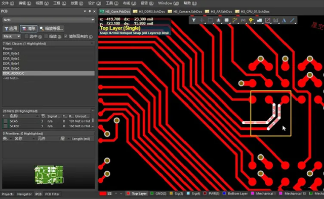
Controlled impedance PCB routing is essential for:
- High-speed digital circuits
- RF and microwave systems
- Differential signal transmission
- High-frequency communication hardware
The characteristic impedance of a PCB transmission line depends on:
- PCB stack-up structure
- Trace width and spacing
- Dielectric material properties
- Copper thickness
- Ground reference configuration
Characteristic impedance can be represented as:
Z0=LCZ_0 = \sqrt{\frac{L}{C}}Z0=CL
Maintaining stable impedance helps:
- Reduce signal reflection
- Improve waveform integrity
- Ensure reliable data transmission
3. Why Controlled Impedance Is Important in PCB Design
Without proper impedance control, high-speed PCB systems may suffer from:
- Signal distortion
- Data transmission errors
- Timing instability
- RF communication degradation
Controlled impedance PCB design improves:
- Signal integrity
- High-speed transmission reliability
- RF system stability
- Electromagnetic compatibility
This is especially important in:
- DDR memory systems
- High-speed networking hardware
- RF communication modules
- Automotive radar electronics
4. Types of Controlled Impedance Structures
4.1 Single-Ended Controlled Impedance
Single-ended impedance routing is commonly used in:
- Clock signals
- RF signal lines
- General high-speed digital routing
The signal trace is referenced to:
- A ground plane
or - A power plane
4.2 Differential Pair Controlled Impedance
Differential routing is widely used in:
- USB interfaces
- PCIe systems
- Ethernet communication
- High-speed serial communication
Differential pair routing improves:
- Noise immunity
- EMI suppression
- Signal stability
4.3 Microstrip and Stripline Structures
Controlled impedance PCB routing commonly uses:
- Microstrip transmission lines
- Stripline transmission lines
These structures help maintain:
- Stable impedance values
- Consistent signal propagation
- Reduced RF signal loss
5. Signal Integrity in Impedance Controlled PCB
Signal integrity is one of the primary goals of impedance controlled PCB design.
Proper impedance control helps reduce:
- Reflection loss
- Ringing effects
- Crosstalk interference
- Timing skew
Signal integrity optimization techniques include:
- Differential pair matching
- Reference plane continuity
- Via optimization
- Short routing paths
- Controlled layer transitions
At KKPCB, advanced PCB routing techniques improve:
- High-speed communication reliability
- RF transmission quality
- Stable system performance
6. PCB Stack-Up Design for Controlled Impedance
Multilayer stack-up design directly affects:
- Characteristic impedance
- Signal integrity
- EMI suppression
- Power integrity
Important stack-up considerations include:
- Dielectric thickness control
- Ground plane positioning
- Layer symmetry
- RF signal isolation
Optimized multilayer PCB structures improve:
- Crosstalk reduction
- Stable impedance consistency
- High-frequency transmission quality
7. PCB Materials for Impedance Controlled PCB
Material selection strongly influences:
- Dielectric performance
- Signal attenuation
- High-frequency stability
Common impedance controlled PCB materials include:
- High Tg FR4
- Low-loss FR4
- Rogers RF laminates
- PTFE-based materials
- Hydrocarbon ceramic substrates
Important material properties include:
- Stable dielectric constant
- Low dissipation factor
- Reliable thermal performance
8. EMI and EMC Optimization in Impedance Controlled PCB
Improper impedance routing can increase:
- Electromagnetic radiation
- RF interference
- Noise coupling
EMI suppression strategies include:
- Ground via stitching
- Controlled return current paths
- Shielding structures
- Differential routing optimization
- Proper layer isolation
These techniques improve:
- EMC compliance
- Signal quality
- RF communication stability
9. Thermal Management in Impedance Controlled PCB
High-speed and RF systems often generate substantial heat.
Thermal management techniques include:
- Thermal via arrays
- Copper heat-spreading planes
- Heat sink integration
- Hybrid multilayer thermal structures
Efficient thermal design improves:
- Signal stability
- Electrical consistency
- Long-term reliability
10. Manufacturing Challenges of Impedance Controlled PCB
Impedance controlled PCB fabrication requires extremely tight manufacturing control.
Key manufacturing challenges include:
- Precise dielectric thickness management
- Accurate trace geometry control
- Stable copper etching quality
- Multilayer alignment precision
- Tight impedance tolerance verification
At KKPCB, advanced manufacturing technologies ensure:
- Stable impedance consistency
- Reliable high-frequency performance
- Accurate multilayer PCB fabrication quality
11. Applications of Impedance Controlled PCB
Impedance controlled PCB technology is widely used in:
- 5G communication systems
- RF and microwave electronics
- AI servers and data centers
- Automotive radar modules
- Aerospace communication systems
- High-speed networking equipment
- Medical imaging systems
These applications require:
- Stable signal integrity
- Low-loss transmission
- Reliable high-speed communication
12. Future Trends in Impedance Controlled PCB Technology
Future impedance controlled PCB development focuses on:
- mmWave communication systems
- Ultra-low-loss PCB materials
- AI-driven high-speed computing
- Advanced HDI PCB integration
- Higher multilayer routing density
Emerging technologies require:
- Faster data transmission
- Lower signal loss
- Better EMI suppression
- More accurate impedance control capability
13. Conclusion
Impedance Controlled PCB technology is essential for modern:
- High-speed digital electronics
- RF communication systems
- Microwave PCB applications
Through optimized:
- Controlled impedance routing
- Signal integrity engineering
- Multilayer PCB stack-up design
- EMI suppression
- Advanced manufacturing precision
engineers can achieve:
- Stable high-speed transmission
- Better RF communication quality
- Reduced signal loss
- Higher system reliability
With extensive expertise in high-frequency PCB engineering and controlled impedance manufacturing, KKPCB delivers advanced PCB solutions for next-generation communication and high-speed electronic systems.
