1. Why High Speed PCB Technology Is Essential
Modern electronic systems are evolving rapidly toward:
- Faster data transmission rates
- Higher operating frequencies
- Greater circuit integration density
- AI-driven computing platforms
- High-bandwidth communication systems
Applications such as:
- 5G infrastructure
- AI servers
- Data centers
- High-performance computing
- Automotive radar systems
- High-speed networking equipment
require PCB designs capable of maintaining stable signal transmission at extremely high speeds.
Traditional PCB design methods are no longer sufficient for handling:
- High-frequency signal integrity
- Electromagnetic interference (EMI)
- Timing synchronization
- Power integrity challenges
As a result, High Speed PCB technology has become critical for modern advanced electronics.
At KKPCB, high-speed PCB solutions are optimized for:
- Stable high-frequency transmission
- Controlled impedance routing
- Low-loss multilayer PCB structures
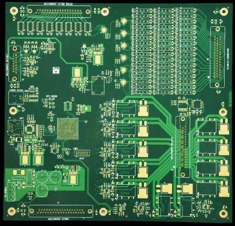
2. What Is a High Speed PCB?
A High Speed PCB is a printed circuit board specifically designed to support:
- High-frequency signal transmission
- Fast digital communication
- Controlled impedance routing
- Low signal loss performance
High-speed PCB systems typically operate with:
- High clock frequencies
- Fast edge-rate signals
- High-density interconnect structures
These PCB designs are widely used in:
- AI computing hardware
- DDR memory systems
- High-speed communication equipment
- RF and microwave electronics
- Data networking systems
3. Key Challenges in High Speed PCB Design
3.1 Signal Integrity Issues
At high transmission speeds, signal integrity becomes one of the most critical design concerns.
Problems include:
- Signal reflection
- Crosstalk
- Insertion loss
- Timing skew
- Return loss
Poor signal integrity can cause:
- Data transmission errors
- Reduced communication reliability
- System instability
3.2 Electromagnetic Interference (EMI)
High-speed switching signals generate significant EMI.
Without proper PCB design:
- Noise coupling increases
- RF interference worsens
- Communication quality degrades
EMI control is essential for:
- Stable system operation
- Regulatory compliance
- Reliable communication performance
3.3 Power Integrity Challenges
High-speed processors and communication ICs require:
- Stable voltage delivery
- Low power noise
- Fast transient response
PCB power distribution networks must minimize:
- Voltage ripple
- Ground bounce
- Switching noise
3.4 Thermal Management
High-speed electronic systems generate substantial heat due to:
- High processing density
- Fast switching frequencies
- High power consumption
Thermal management directly impacts:
- Signal stability
- Reliability
- Product lifespan
4. Controlled Impedance in High Speed PCB
Controlled impedance is one of the most important principles in high-speed PCB design.
Proper impedance control helps:
- Reduce signal reflection
- Improve transmission quality
- Maintain waveform integrity
Common controlled impedance structures include:
- Microstrip routing
- Stripline routing
- Differential pair routing
At KKPCB, impedance-controlled multilayer stack-up design ensures stable high-speed signal performance.
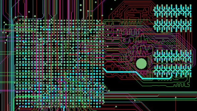
5. Signal Integrity Optimization Techniques
High-speed PCB signal integrity optimization includes:
- Short routing paths
- Differential pair matching
- Reference plane continuity
- Via optimization
- Return path management
These techniques improve:
- Signal stability
- Timing accuracy
- Data transmission reliability
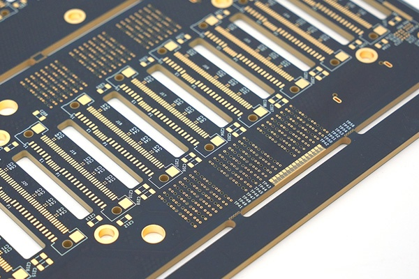
6. PCB Stack-Up Design for High Speed PCB
Multilayer stack-up design plays a critical role in:
- Signal integrity
- EMI suppression
- Power integrity
Proper stack-up design includes:
- Dedicated ground planes
- Controlled dielectric thickness
- Symmetrical layer structures
- Power plane optimization
Optimized stack-up improves:
- Crosstalk reduction
- Signal isolation
- High-frequency stability
7. High Speed PCB Materials
Material selection greatly affects high-speed signal performance.
Common high-speed PCB materials include:
- Low-loss FR4
- Rogers high-frequency laminates
- PTFE-based materials
- Hydrocarbon ceramic laminates
Key material properties include:
- Low dissipation factor
- Stable dielectric constant
- High thermal reliability
Low-loss PCB materials help reduce:
- Signal attenuation
- Timing distortion
- RF transmission loss
8. EMI Control in High Speed PCB Design
EMI suppression techniques include:
- Ground via stitching
- Shielding structures
- Differential routing
- Controlled return current paths
- Proper layer isolation
These methods improve:
- Signal integrity
- RF noise suppression
- System stability
9. Thermal Management in High Speed PCB
Thermal management techniques include:
- Thermal via arrays
- Copper heat-spreading planes
- Heat sink integration
- High thermal conductivity materials
Efficient thermal design improves:
- Processing stability
- Signal consistency
- Long-term reliability
10. Manufacturing Challenges of High Speed PCB
High-speed PCB fabrication requires extremely tight manufacturing control.
Key challenges include:
- Impedance tolerance accuracy
- Precise layer registration
- Stable dielectric thickness
- Low-profile copper processing
- High-density multilayer alignment
At KKPCB, advanced PCB manufacturing technologies ensure:
- Stable electrical performance
- High-frequency reliability
- Consistent multilayer PCB quality
11. Applications of High Speed PCB
High Speed PCBs are widely used in:
- AI servers and data centers
- 5G communication infrastructure
- High-speed networking equipment
- Automotive radar systems
- Aerospace electronics
- High-performance computing systems
- Medical imaging equipment
These systems require:
- Ultra-fast data transmission
- Stable signal integrity
- Reliable power delivery
12. Future Trends in High Speed PCB Technology
Future high-speed PCB development focuses on:
- AI-driven computing systems
- 800G and higher networking platforms
- Advanced HDI PCB integration
- mmWave communication systems
- Ultra-low-loss PCB materials
Emerging technologies require:
- Higher transmission bandwidth
- Lower latency
- Greater signal integrity precision
- More compact multilayer PCB structures
13. Conclusion
High Speed PCB technology is essential for modern:
- High-frequency communication systems
- AI computing platforms
- High-bandwidth digital electronics
Through optimized:
- Signal integrity engineering
- Controlled impedance routing
- EMI suppression
- Thermal management
- Advanced multilayer PCB manufacturing
engineers can achieve:
- Faster data transmission
- Better communication stability
- Higher system reliability
With extensive expertise in high-frequency PCB engineering, KKPCB delivers reliable PCB solutions for next-generation high-speed electronic systems.
