multilayer PCB - KKPCB
 
HomeTag

multilayer PCB - KKPCB

BT Epoxy PCB: High-Performance Substrates for IC Packaging and High-Speed Design

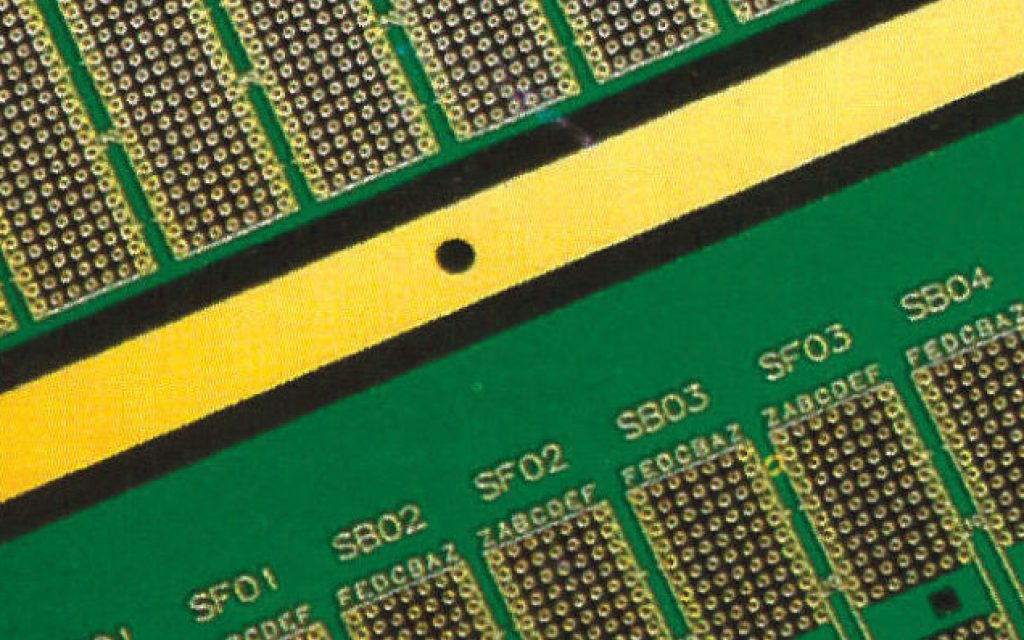
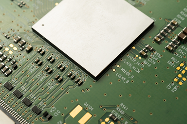
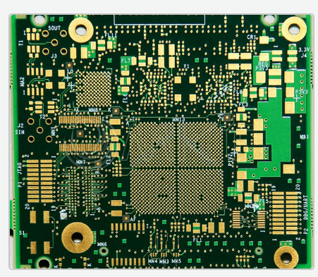
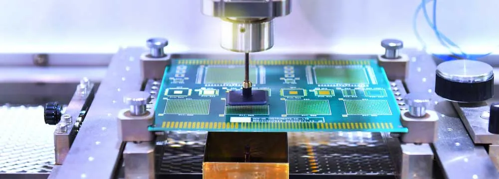
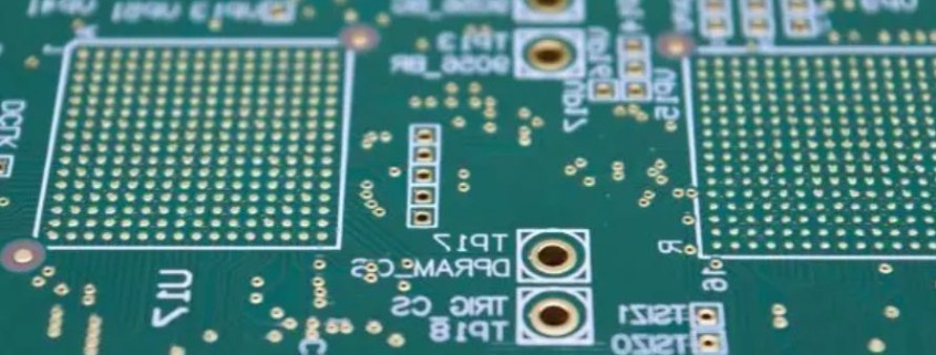
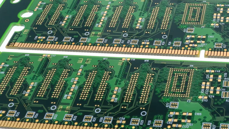
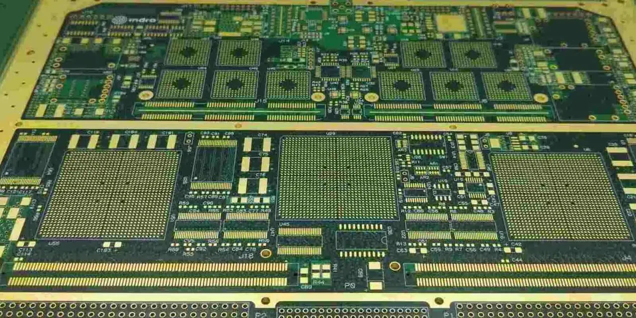
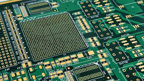
What Is a BT Epoxy PCB? A BT Epoxy PCB is a high-performance PCB built using BT epoxy resin (Bismaleimide-Triazine), a material widely used in IC substrate and semiconductor packaging applications. Compared to standard FR-4, a BT Epoxy PCB offers: Higher glass transition temperature (Tg) Lower dielectric loss Better dimensional stability Improved reliability under thermal...

Fine Line PCBs: Pushing the Limits of Precision and Density in Modern Electronics

What Is a Fine Line PCB? A Fine Line PCB refers to a board manufactured with extremely narrow trace width and spacing, typically: ≤100 µm (4 mil) → standard fine line ≤75 µm (3 mil) → advanced ≤50 µm (2 mil) or below → ultra-fine line These geometries go beyond conventional PCB fabrication limits and...

Microvia PCBs: Design, Reliability, and Engineering Trade-Offs Explained

Why Microvias Are Critical in Modern PCB Design As electronic devices continue to shrink while performance demands increase, traditional through-hole vias become a limiting factor. Microvias solve this by enabling high-density interconnects with shorter electrical paths. They are essential when: BGA pitch ≤ 0.8 mm (especially ≤ 0.5 mm) Routing congestion limits layout feasibility High-speed...

HDI PCBs Explained: Stack-Up Choices, Via Strategies, and Cost Trade-Offs

What Actually Defines an HDI PCB? An HDI PCB (High-Density Interconnect PCB) is not defined by layer count alone, but by how efficiently interconnections are implemented. The key differentiators are: Microvias (laser-drilled vias) Blind and buried vias Fine line and spacing (typically ≤100 µm) High connection density per unit area The goal of HDI is...

High Pin Count PCBs: Managing Complexity in Advanced Electronic Systems

System Complexity as the Driving Force Modern electronic systems are no longer defined by individual components, but by highly integrated devices with massive I/O requirements. CPUs, GPUs, FPGAs, and advanced SoCs now feature hundreds to thousands of pins, driving the need for High Pin Count PCBs. This shift introduces a new level of complexity: Multiple...

HDI PCBs: High-Density Interconnect Solutions for Next-Generation Electronics

Why HDI PCBs Are No Longer Optional As electronic devices become smaller, faster, and more complex, traditional multilayer PCB designs struggle to keep up. HDI (High-Density Interconnect) PCBs address this challenge by enabling higher routing density, shorter signal paths, and better electrical performance. At the core of HDI technology is the use of: Microvias (laser-drilled...

High Pin Count PCBs: Enabling Complex Interconnections in Advanced Electronics

Why High Pin Count Matters As modern electronic systems evolve, integrated circuits such as CPUs, GPUs, FPGAs, and high-speed SoCs demand hundreds or even thousands of I/O connections. A High Pin Count PCB is designed to support these devices by enabling dense interconnections within limited board space. Unlike standard PCB designs, high pin count boards...

Probe Card PCBs: Precision Platforms for Semiconductor Testing

What Makes Probe Card PCBs Unique A Probe Card PCB is not a typical circuit board—it is a high-precision interface platform used in semiconductor wafer testing. It connects test equipment (ATE) to microscopic pads on silicon wafers through probe needles or MEMS structures. Unlike standard PCBs, probe card boards must support: Ultra-fine pitch interconnections High...

Buried Via PCBs: Strategic Layer Interconnects for High-Performance Designs

Why Buried Vias Matter As electronic systems become more compact and performance-driven, traditional via structures are no longer sufficient for complex routing requirements. A Buried Via PCB enables connections only between internal layers, eliminating unnecessary vertical paths through the entire board. This design approach is not just about saving space—it is about engineering control over...

High Layer Count PCBs: Advanced Solutions for Complex Electronic Systems

A High Layer Count PCB is a printed circuit board with 8 or more signal layers, often extending to 20–40 layers or more in advanced systems. These boards enable dense routing, compact design, and integration of multiple high-speed and RF circuits in a single assembly. High layer count PCBs are critical in: High-performance computing Networking...