HomeTag

mmWave PCB - KKPCB

Optimize Dielectric Stability and Low-Df Transmission with Duroid 5880 PCB Architectures for 10–67 GHz RF Subsystems

RF subsystems operating from 10 to 67 GHz—spanning 5G mmWave, satellite links, and aerospace communication modules—demand ultra-stable dielectric properties and minimal signal loss. Any Dk/Df variation or thermal-induced impedance drift directly degrades signal integrity, phase coherence, and overall RF system efficiency. Duroid 5880 PCB laminates (Dk = 2.2 ± 0.02, Df = 0.0009 @10 GHz)...
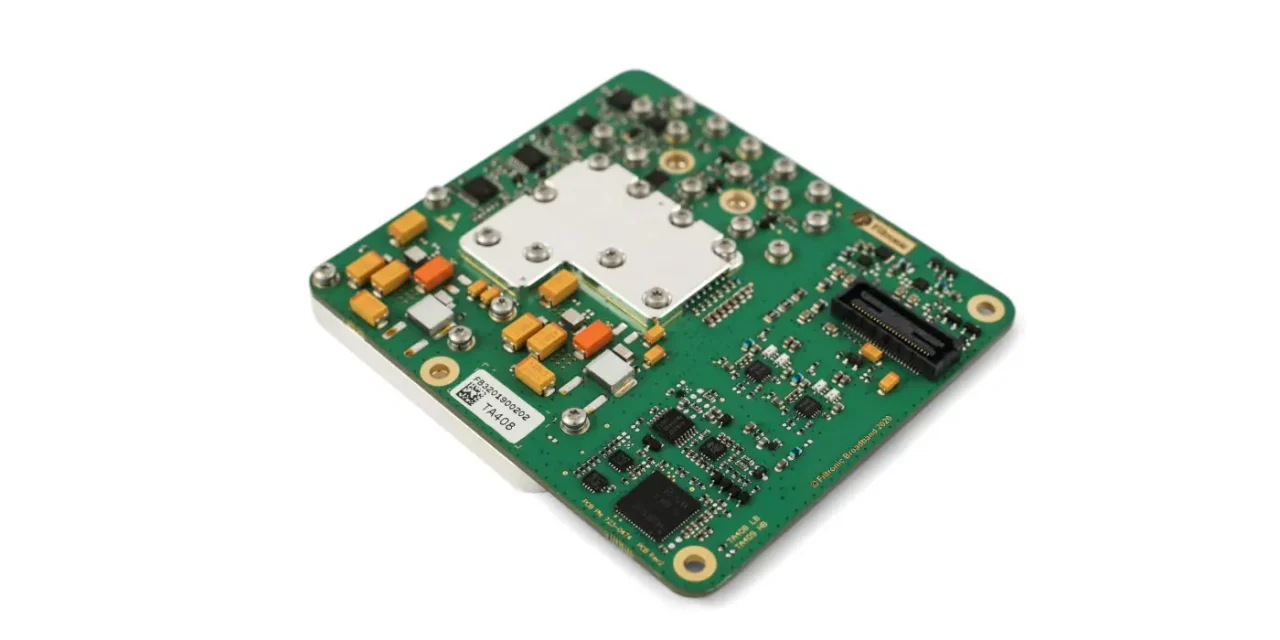
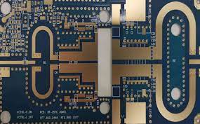
mmWave Module PCB Engineering: Material Precision, RF Loss Control, and Manufacturing Realities

Next-generation RF transceivers—whether for 5G mmWave, SATCOM terminals, phased-array antennas, or short-range high-bandwidth links—place brutal demands on PCB materials. To maintain ultra-low insertion loss, wideband consistency, stable phase response, and clean radiation efficiency, mmWave module PCB materials must deliver precision alignment, ultra-low dielectric loss, tight Dk control, and minimal copper roughness across every layer. In...

Maximize High-Frequency Signal Integrity with Low Loss PCB Laminates in 5G mmWave Antenna Systems

High-frequency signal integrity is the defining performance factor in modern 5G mmWave antenna systems, where routing density, insertion loss, and phase stability determine overall RF efficiency. As 5G architectures transition to 26–29 GHz, 37–40 GHz, and 60 GHz mmWave bands, the electrical behavior of the Low Loss PCB stackup becomes just as important as the...

Optimize Thermal Performance and EMI Suppression in High-Density RF Modules with Low Loss PCB Materials

High-density RF modules used in 5G radios, SATCOM terminals, phased-array beamformers, and mmWave front-end units are increasingly constrained by thermal stress, EMI coupling, and insertion loss. As operating frequencies push beyond 10–40 GHz, traditional FR-4 structures can no longer maintain stable impedance, consistent dielectric behavior, or low-loss routing. This is where Low Loss PCB materials—such...

mmWave Module PCB Engineering for High-Frequency, Low-Loss and Thermally Stable RF Front-End Systems

The shift toward 5G FR2, advanced radar, high-resolution sensing and satellite communication has placed intense performance pressure on mmWave Module PCB design. At frequencies from 24 GHz to 86 GHz, the PCB is no longer a passive carrier—it becomes an active RF component whose materials, stackup, via transitions and routing geometries directly dictate performance. A...

Maximize RF Channel Integrity and Minimize Signal Loss with Blind Via PCB Architectures for High-Speed Communication Modules

High-speed communication modules in 5G, satellite transceivers, and high-frequency computing systems demand extreme precision in signal routing and interconnect integrity. As layer density increases and modules become more compact, traditional through-hole vias introduce unwanted parasitic effects, signal reflection, and EMI interference, compromising both channel fidelity and system performance. Blind via PCB technology enables selective inter-layer...

Optimize RF Transmission and Phase Consistency Using High-Frequency Sensor PCB Laminates in Automotive ADAS Sensing Modules

The Role of High-Frequency PCB in Automotive ADAS Sensing Systems Next-generation automotive ADAS (Advanced Driver Assistance Systems) rely on high-performance sensing technologies, including 77–81 GHz radar, LiDAR, and mmWave sensor arrays, to achieve accurate object detection, adaptive cruise control, collision avoidance, and autonomous driving functions. At these high frequencies, PCB performance directly affects radar accuracy...

Enhance Thermal Reliability and High-Power RF Efficiency Through Advanced 5G Router PCB Stackups

5G router PCB platforms operate under multi-band RF loads, high-density routing, and continuous thermal cycling in compact CPE enclosures. Achieving stable RF efficiency requires a stackup engineered around low-loss materials, controlled dielectric stability, and carefully optimized thermal paths. This article analyzes how engineered 5G router PCB stackups improve RF efficiency, insertion-loss performance, and long-term thermal...

Low Loss PCBs Explained: Materials, Features & High-Frequency Performance

What Is a Low Loss PCB? Premium Materials, Performance Advantages & Applications In high-frequency electronics, signal integrity is everything. As data rates climb and RF systems move into the mmWave range, traditional FR-4 PCBs quickly become inadequate due to excessive dielectric loss, copper loss and thermal instability. At KKPCB, we engineer Low Loss PCBs specifically...

RF PCB Design for 5G Devices: Antenna Integration, Impedance Control & High-Frequency Layout Guide

RF PCB Design for 5G Devices: High-Frequency Architecture, Antenna Integration & Engineering Best Practices Designing RF PCBs for 5G hardware is far more than simple high-speed layout—it requires a deep command of electromagnetic behavior, antenna engineering, high-frequency signal routing, impedance control, and noise isolation.In next-generation wireless systems, the antenna is no longer a passive component—it...