
The Role of High-Frequency PCB in Automotive ADAS Sensing Systems
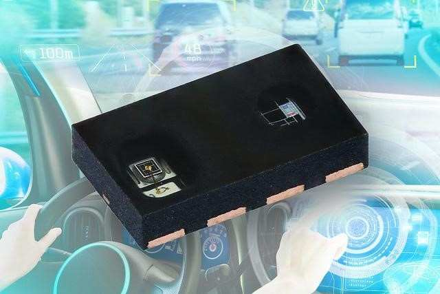
Next-generation automotive ADAS (Advanced Driver Assistance Systems) rely on high-performance sensing technologies, including 77–81 GHz radar, LiDAR, and mmWave sensor arrays, to achieve accurate object detection, adaptive cruise control, collision avoidance, and autonomous driving functions.
At these high frequencies, PCB performance directly affects radar accuracy and system reliability. Automotive ADAS Radar PCBs must provide stable dielectric performance, low insertion loss, precise impedance control, and phase-consistent RF transmission while operating under demanding vehicle environments involving thermal cycling, vibration, and humidity.
A high-quality high-frequency sensor PCB enables reliable mmWave signal propagation, minimizes electromagnetic interference (EMI), and maintains consistent RF performance throughout the product lifecycle.
Key Engineering Challenges in Automotive ADAS Radar PCB Design
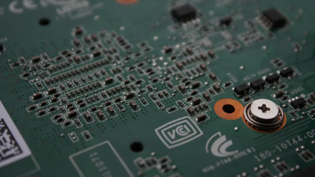
1. mmWave Signal Loss and RF Transmission Stability
At 77–81 GHz operating frequencies, even minor material variations and manufacturing inconsistencies can significantly affect RF performance.
Common challenges include:
- Dielectric loss from substrate materials
- Copper surface roughness impact
- Signal attenuation in transmission paths
- Reduced signal-to-noise ratio (SNR)
To overcome these challenges, ADAS Radar PCBs require:
- Low-loss RF laminates
- Stable dielectric constant (Dk)
- Ultra-low dissipation factor (Df)
- Optimized RF trace structures
These design considerations help maintain signal strength and improve radar detection accuracy.
2. Phase Stability Under Automotive Temperature Variations
Automotive radar systems rely on precise phase relationships for beamforming and target detection. Temperature fluctuations can introduce phase deviation if PCB materials are not properly controlled.
Major factors include:
- Thermal expansion mismatch between copper and laminate
- Dielectric constant variation with temperature
- Mechanical stress during thermal cycling
Reliable designs require:
- Controlled coefficient of thermal expansion (CTE)
- Stable Dk/Df characteristics
- Precision multilayer stack-up design
Maintaining phase stability helps prevent beamforming errors and improves sensing accuracy.
3. EMI Control in Dense mmWave Sensor Layouts
Modern ADAS modules integrate multiple RF channels, antennas, processors, and power circuits into compact spaces.
Potential EMI issues include:
- Crosstalk between RF channels
- Insufficient grounding
- Uncontrolled return paths
- Interference from nearby circuits
Effective mitigation strategies include:
- Optimized ground plane design
- Embedded shielding vias
- RF isolation structures
- Controlled routing geometry
These techniques improve electromagnetic compatibility and reduce false detection risks.
4. Mechanical and Environmental Reliability
Automotive PCBs must withstand harsh operating conditions, including vibration, temperature cycling, and moisture exposure.
Key reliability requirements include:
- Resistance to thermal stress
- Strong layer bonding
- Low moisture absorption
- Prevention of delamination and microcracks
Material stability and manufacturing precision are essential for long-term ADAS sensor reliability.
High-Frequency PCB Material Considerations for ADAS Applications
Material selection is one of the most important factors affecting mmWave PCB performance.
Typical high-frequency laminate characteristics include:
| Parameter | Engineering Importance |
|---|---|
| Stable Dk | Maintains consistent impedance and RF phase performance |
| Low Df | Reduces insertion loss at high frequencies |
| Controlled CTE | Minimizes phase drift during thermal cycling |
| Low Moisture Absorption | Maintains dielectric stability in humid environments |
| High Thermal Conductivity | Improves heat dissipation in compact sensor modules |
Compared with conventional FR-4 materials, high-frequency RF laminates provide better electrical consistency and lower signal loss for automotive radar and mmWave sensing applications.
KKPCB Engineering Case Study:77GHz Automotive Radar Sensor PCB
Project Background
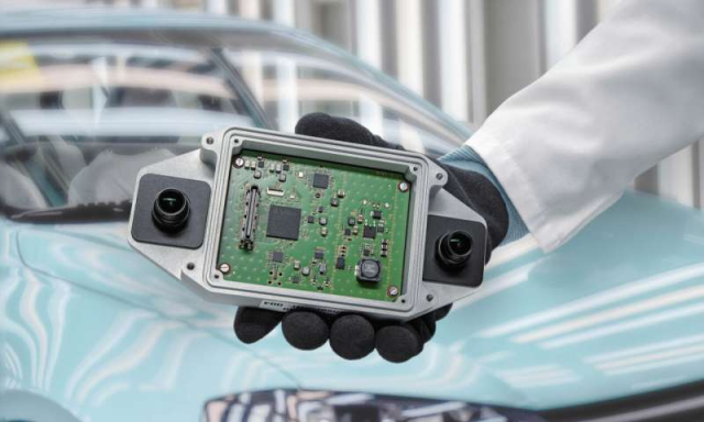
A Tier-1 automotive supplier required a 6-layer radar sensor PCB for a 77 GHz ADAS application. The design target included:
- Phase deviation below 0.5°
- Insertion loss below 0.35 dB/in
- Stable RF performance under thermal and mechanical stress
The main challenges included maintaining RF phase consistency, reducing signal loss, and ensuring long-term reliability in automotive environments.
KKPCB Engineering Solutions
High-Frequency Material Selection
- Applied high-frequency RF laminate for critical signal layers
- Optimized dielectric thickness for RF performance
RF Stack-up Optimization
- Developed hybrid 6-layer PCB stack-up
- Utilized low-roughness copper for improved high-frequency transmission
- Controlled dielectric thickness variation through precision lamination
Signal Integrity and EMI Optimization
- Added embedded TDR calibration structures
- Optimized ground plane segmentation
- Applied shielding via structures to improve RF isolation
Thermal Reliability Enhancement
- Optimized copper distribution and thermal paths
- Improved heat dissipation around high-power areas
Performance Validation Results
| Parameter | Target | Result |
|---|---|---|
| Insertion Loss @77 GHz | <0.35 dB/in | 0.30 dB/in |
| Phase Deviation | <0.5° | 0.42° |
| EMI Reduction | >30% | 35% |
| Impedance Variation | ±3% | ±1.6% |
RF Simulation and Manufacturing Verification
To ensure design reliability, the project included:
RF Simulation
- HFSS modeling for microstrip and stripline optimization
- Reduced inter-layer coupling and signal interference
Electrical Verification
- ADS/TDR analysis for impedance and phase consistency
- Maintained phase linearity across 77–81 GHz channels
Thermal Analysis
- FEM simulation to optimize heat distribution
- Reduced hotspot temperature by 4.5°C
Manufacturing Control
- AOI inspection and solder reflow monitoring
- Maintained alignment accuracy within ±10 μm
Environmental Reliability Testing
| Test | Condition | Result |
|---|---|---|
| Thermal Cycling | -40°C to +125°C,1000cycles | Phase deviation <0.5°, no delamination |
| Vibration & Shock | 5–500 Hz, 10G | No microcracks or solder fatigue |
| Humidity Testing | 85°C /85%RH,1000 h | Stable Dk/Df performance |
| Solder Reflow | 260°C ×3 cycles | No warpage |
| EMI Evaluation | Dense mmWave routing | Crosstalk reduced 35% |
Conclusion: Enabling Reliable mmWave Performance for Automotive ADAS
Automotive ADAS Radar PCBs require advanced RF engineering, precise material control, and reliable manufacturing processes to support next-generation sensing technologies.
Through optimized high-frequency materials, hybrid stack-up design, impedance control, EMI mitigation, and precision fabrication, high-performance ADAS PCBs can achieve stable mmWave transmission, accurate radar detection, and long-term automotive reliability.
KKPCB supports automotive electronics development through RF PCB engineering, high-frequency material solutions, stack-up optimization, impedance verification, and manufacturing process control, helping customers build reliable radar and sensor platforms for advanced mobility applications.

