
HomeTag

High-Speed PCB Layout - KKPCB

Minimize Crosstalk and Maintain Impedance Precision Using Advanced Blind Via PCB Layouts in 5G mmWave Systems

5G mmWave hardware doesn’t leave much room for layout mistakes. When operating above 24 GHz, a few microns of misalignment, a poorly shaped via stub, or an uncontrolled dielectric transition can collapse RF integrity. That is why advanced blind via PCB layouts have become a core enabling technology for minimizing crosstalk, stabilizing impedance, and preserving...
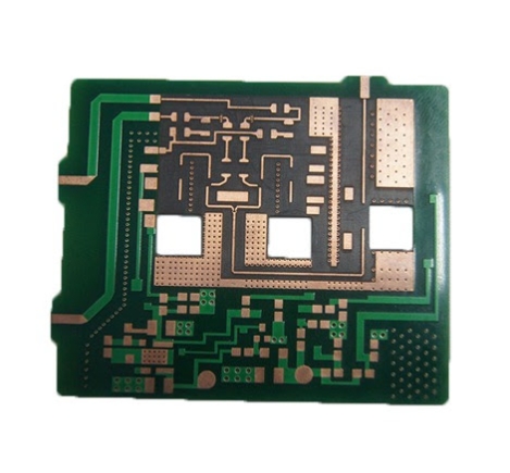
RF PCB Design for 5G Devices: Antenna Integration, Impedance Control & High-Frequency Layout Guide

RF PCB Design for 5G Devices: High-Frequency Architecture, Antenna Integration & Engineering Best Practices Designing RF PCBs for 5G hardware is far more than simple high-speed layout—it requires a deep command of electromagnetic behavior, antenna engineering, high-frequency signal routing, impedance control, and noise isolation.In next-generation wireless systems, the antenna is no longer a passive component—it...

High-Speed PCB Design Guide 5: Noise Reduction Technology for DSP Systems

Digital Signal Processors (DSPs) are widely used in applications that require high-speed data processing and real-time computation, including industrial automation, wireless communications, medical imaging, radar systems, machine vision, audio processing, and AI edge computing. As DSP clock frequencies and data rates continue to increase, maintaining signal integrity while minimizing system noise has become one of...
