
Digital Signal Processors (DSPs) are widely used in applications that require high-speed data processing and real-time computation, including industrial automation, wireless communications, medical imaging, radar systems, machine vision, audio processing, and AI edge computing. As DSP clock frequencies and data rates continue to increase, maintaining signal integrity while minimizing system noise has become one of the most important challenges in high-speed PCB design.
Noise in a DSP system can originate from switching power supplies, high-speed digital interfaces, clock distribution networks, and poor PCB layout practices. If these noise sources are not properly controlled, they can lead to signal distortion, timing violations, reduced electromagnetic compatibility (EMC), increased bit error rates, and even intermittent system failures.
This article explores the primary sources of noise in DSP-based systems and presents practical PCB design techniques that help improve signal quality, system stability, and manufacturing reliability.
1. Why Noise Control Is Critical in DSP Systems
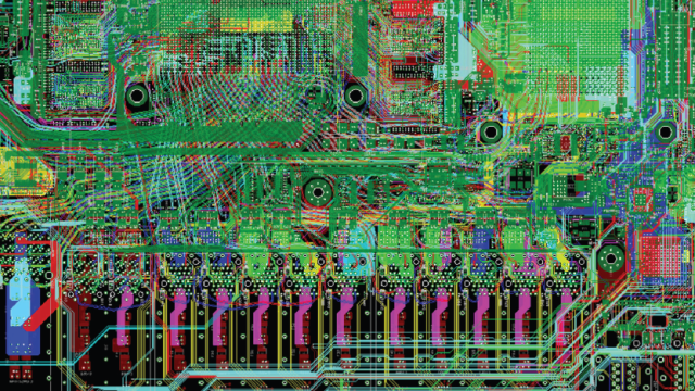
DSP devices typically operate with:
- High-frequency core clocks
- Multiple power domains
- High-speed memory interfaces
- High-speed serial communication buses
- Sensitive analog front-end circuits
Unlike low-speed digital circuits, DSP systems often process large volumes of data with strict timing requirements. Even small amounts of electrical noise can affect:
- Clock stability
- ADC and DAC accuracy
- Data transmission reliability
- Real-time processing performance
Noise reduction should therefore be considered from the earliest stages of PCB design rather than addressed during system debugging.
2. Common Noise Sources in DSP PCB Design
Power Supply Noise
Rapid switching inside DSP cores causes significant transient current demand.
Without adequate power distribution design, this may result in:
- Supply voltage ripple
- Ground bounce
- Timing instability
- Increased electromagnetic emissions
Power integrity becomes increasingly important as operating frequencies rise.
Clock Signal Noise
Clock signals are often the highest-frequency signals on the PCB.
Poor clock routing may introduce:
- Jitter
- Reflection
- Crosstalk
- Excessive EMI radiation
Since the DSP relies on precise timing, clock instability can affect the entire system.
Crosstalk Between High-Speed Signals
Closely spaced parallel traces may create capacitive and inductive coupling.
Common examples include:
- DDR memory buses
- LVDS interfaces
- High-speed SPI
- Ethernet
- PCIe
Crosstalk can lead to:
- False switching
- Timing errors
- Signal distortion
Switching Noise
High-speed digital outputs generate large transient currents during logic transitions.
These switching events produce:
- Simultaneous Switching Output (SSO) noise
- Ground bounce
- Power supply fluctuations
The effect becomes more pronounced when many output pins switch simultaneously.
External EMI
DSP systems operating near:
- Motor drives
- Switching power supplies
- RF transmitters
- High-current circuits
may experience electromagnetic interference that couples into sensitive signal paths.
3. PCB Stack-Up Design for Noise Reduction
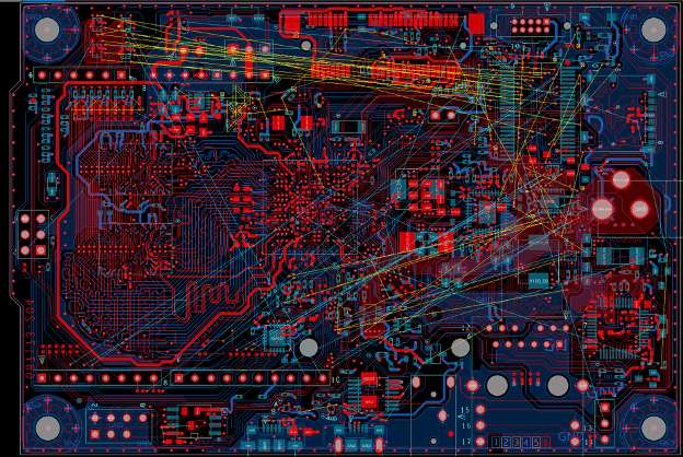
A well-designed PCB stack-up is the foundation of low-noise DSP systems.
Recommended practices include:
- Continuous ground planes adjacent to signal layers
- Dedicated power planes for critical voltage rails
- Controlled impedance routing for high-speed signals
- Short return current paths
Separating high-speed signal layers from noisy power routing helps reduce EMI and improves signal integrity.
4. Power Distribution Network (PDN) Optimization
Power integrity directly affects DSP performance.
Effective PDN design includes:
Proper Decoupling Capacitor Placement
Place decoupling capacitors:
- As close as possible to each DSP power pin
- With short, low-inductance connections
- Connected directly to the ground plane through dedicated vias
Using multiple capacitor values helps suppress noise across a broad frequency range.
Separate Analog and Digital Power
If the DSP includes analog functions such as ADCs or DACs:
- Separate analog and digital power supplies where recommended by the device manufacturer.
- Connect analog and digital grounds using an appropriate grounding strategy rather than allowing uncontrolled current paths.
Minimize Power Loop Area
Reducing loop inductance improves transient response and lowers radiated emissions.
Power and ground paths should remain tightly coupled throughout the PCB.
5. Clock Routing Best Practices
The clock network is one of the most sensitive parts of a DSP PCB.
Recommended design techniques include:
- Keep clock traces as short as possible.
- Avoid unnecessary vias.
- Route over continuous reference planes.
- Maintain controlled impedance where required.
- Avoid routing near switching power circuits.
Clock traces should not be routed in parallel with noisy digital buses for long distances.
6. High-Speed Signal Routing Techniques
Controlled Impedance
High-speed DSP interfaces often require impedance-controlled routing to minimize reflections and ensure signal integrity.
Typical interfaces include:
- DDR memory
- Ethernet
- USB
- PCI Express
- LVDS
Impedance values should match the interface specifications and PCB stack-up.
Length Matching
Signals within high-speed buses should be length matched where required.
Examples include:
- DDR address lines
- Data buses
- Differential pairs
Proper matching reduces timing skew and improves data reliability.
Differential Pair Routing
For differential interfaces:
- Maintain constant spacing.
- Keep both traces equal in length.
- Avoid unnecessary layer changes.
- Preserve symmetry throughout the route.
7. Grounding Strategies
A solid ground structure is essential for reducing DSP system noise.
Best practices include:
- Use continuous ground planes.
- Avoid splitting reference planes beneath high-speed traces.
- Minimize return path discontinuities.
- Reduce ground loop formation.
Ground vias should be placed strategically to provide low-impedance return paths.
8. Component Placement Considerations
Component placement significantly influences overall system noise.
Recommended layout principles include:
- Position the DSP near high-speed memory devices to shorten critical signal paths.
- Place decoupling capacitors adjacent to power pins.
- Keep analog circuits away from switching regulators and high-speed digital interfaces.
- Separate noisy power circuits from sensitive signal-conditioning circuitry.
Good placement often reduces routing complexity while improving overall electrical performance.
9. EMI and EMC Design Techniques
DSP systems frequently require compliance with EMC standards.
Common PCB techniques include:
- Ground stitching vias around board edges
- Proper shielding for sensitive circuits
- Controlled return current paths
- Filtering on external interfaces
- Optimized connector placement
Where necessary, common-mode chokes or ferrite beads may be used to suppress conducted noise on external connections.
10. Thermal Considerations
High-performance DSP devices can dissipate significant power during operation.
Elevated temperatures may increase:
- Electrical noise
- Clock instability
- Component aging
Thermal management techniques include:
- Thermal vias beneath the DSP package
- Large copper planes for heat spreading
- Heat sinks when required
- Proper airflow design
Thermal and electrical design should be considered together to achieve long-term reliability.
11. Manufacturing Considerations
Even an electrically optimized PCB can encounter production issues if manufacturability is overlooked.
A Design for Manufacturability (DFM) review should evaluate:
- High-speed stack-up feasibility
- Controlled impedance capability
- Via structures
- Component spacing
- Assembly tolerances
- Test point accessibility
Early DFM analysis helps reduce production risk while improving yield and consistency.
12. Typical Applications
Noise reduction techniques for DSP-based PCBs are widely applied in:
- Industrial automation controllers
- Machine vision systems
- Medical imaging equipment
- Software-defined radio (SDR)
- Radar signal processing
- Audio and video processing equipment
- AI edge computing platforms
- High-speed data acquisition systems
Each application places different demands on signal integrity, power integrity, and EMI control, but the underlying PCB design principles remain similar.
Conclusion
Noise reduction is a fundamental aspect of high-speed DSP PCB design. As processor frequencies, interface speeds, and system complexity continue to increase, successful PCB designs depend on a combination of sound electrical engineering practices rather than any single optimization technique.
Careful attention to PCB stack-up, power distribution, clock routing, signal integrity, grounding, component placement, EMI control, and thermal management can significantly improve system stability and reliability. Incorporating these considerations early in the design process, together with thorough DFM review and manufacturing validation, helps reduce debugging time, improve first-pass success, and support reliable production of high-performance DSP-based electronic systems.
