HomeTag

HDI PCB - KKPCB

Control of Conductor Etching in PCB Manufacturing: Precision Copper Etching for Fine-Line Circuit Patterns

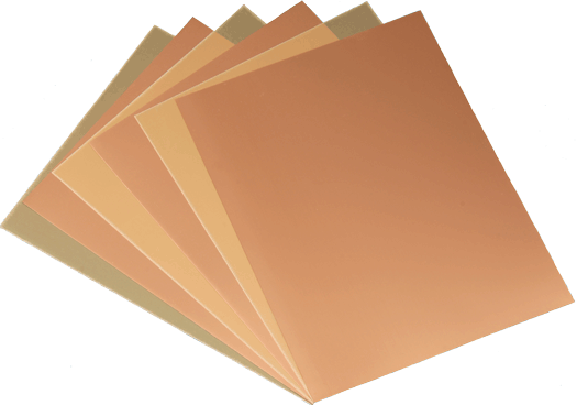
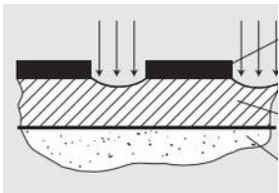
Control of Conductor Etching Process in Printed Circuit Boards Copper etching is one of the most critical steps in printed circuit board (PCB) manufacturing, as it directly determines the accuracy and reliability of conductive circuit patterns. The term “printed circuit board” originates from this process, since etching is the final stage of photolithography used to...
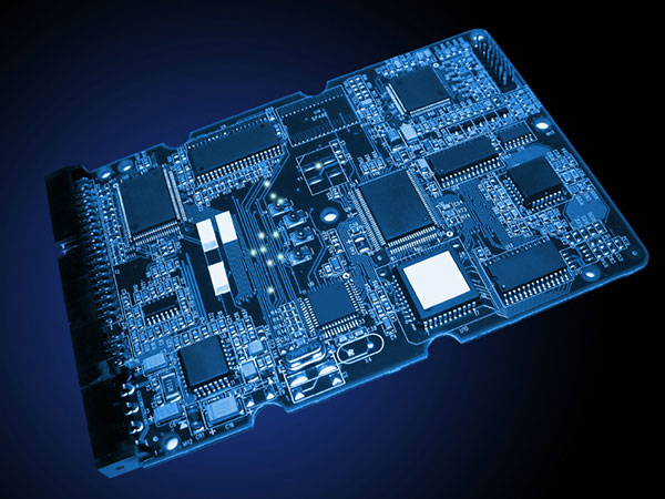
Introduction: PCB Architecture as the Core of Robotics Systems In modern autonomous robotics and industrial robotics, the design of Robotics PCB architecture plays a decisive role in determining system performance, real-time responsiveness, and operational reliability. As robots become more intelligent, compact, and interconnected, the demand for high-density, high-speed, and high-reliability PCB solutions continues to grow....

PCB Prototype Engineering: Achieving High Reliability, High Speed, and High Precision in Modern Electronics

Introduction: Why PCB Prototype Engineering Defines Modern Electronics A PCB Prototype is no longer just a pre-production sample—it is the central engineering stage that determines product performance, manufacturability, reliability, and cost.In advanced electronics such as 5G, IoT, robotics, automotive, aerospace, AI edge computing, and industrial automation, a well-engineered PCB Prototype ensures signal integrity, thermal stability,...

Boost Design Accuracy and Signal Integrity Using High-Precision PCB Prototype Fabrication Technologies

High-precision PCB prototype fabrication has become the backbone of modern electronics development. As product cycles shrink and system complexity rises—spanning RF modules, high-speed digital interfaces, IoT sensors, EV power systems, and aerospace electronics—the demand for PCB prototype accuracy, signal integrity stability, and manufacturing predictability has never been higher. A high-reliability prototype is not “just a...

Medical PCB Solutions: High-Reliability Printed Circuit Boards for Healthcare & Life-Saving Devices

Medical PCB Solutions: Precision, Reliability, and Safety in Healthcare Electronics 1. Introduction: The Evolution of Medical Electronics As modern medicine continues to embrace digital transformation, Printed Circuit Boards (PCBs) have become the silent foundation behind every advanced healthcare device.From portable monitors to implantable electronics, medical-grade PCBs ensure accuracy, safety, and reliability in life-critical applications. At...

Industrial IoT PCB Innovation: The Core of Intelligent Manufacturing

Industrial IoT PCB Innovation: The Core of Intelligent Manufacturing 1. Introduction: The Intelligent Backbone of Industry 4.0 The Industrial Internet of Things (IIoT) represents the convergence of machines, sensors, and intelligent electronics into a unified, connected ecosystem. By enabling seamless communication between devices and systems, IIoT is transforming traditional manufacturing into smart, self-optimizing environments. At...

Probe Card PCB: Engineering Precision for High-Accuracy Wafer-Level Semiconductor Testing

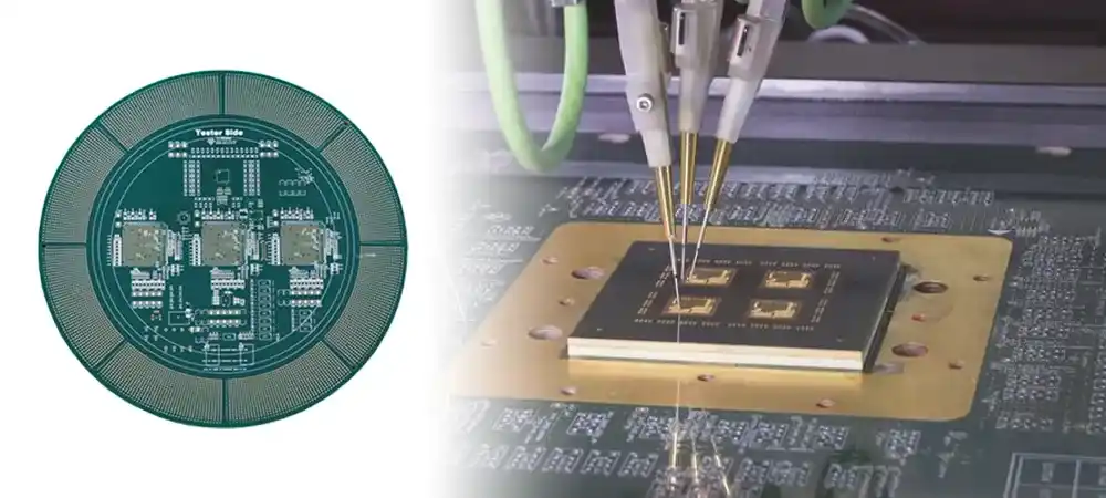
Probe Card PCB: Engineering Precision for Wafer-Level Testing Introduction At the wafer-level test stage, the probe card PCB serves as the indispensable interface between automated test equipment (ATE) and the semiconductor wafer. As device geometries continue shrinking and electrical performance requirements become more demanding, precision test interfaces have become essential. The probe card PCB establishes...

Engineering Biomedical PCBs: Precision, Reliability, and Innovation by KKPCB

Engineering Biomedical PCBs for the Future of Healthcare   In modern healthcare, technology isn’t just an assistant—it’s an extension of human capability. Every medical innovation, from life-sustaining implants to AI-powered diagnostic equipment, relies on one silent enabler: the Printed Circuit Board (PCB). At KKPCB, we design and manufacture biomedical PCBs that meet the uncompromising demands...

Blind and Buried Vias in PCB Design – Advanced HDI Interconnection Solutions

Blind and Buried Vias in PCB Design — Structure, Function, and Manufacturing Insights As the miniaturization of electronic components continues to accelerate, PCB designs must accommodate finer pitch components and higher circuit densities, especially in advanced mobile, communication, and computing applications. One of the critical technologies enabling this evolution is the use of blind and...