
HomeTag

RF layout - KKPCB

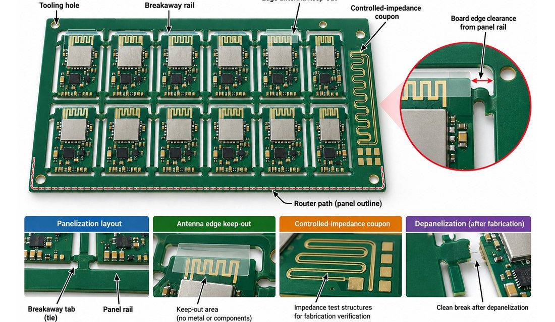
Why a Zigbee PCB Passes Layout Review but Fails at Panelization

Table of Contents Treat the panel as an RF state Protect the antenna edge and return path Control tabs, rails, and depanelization Release evidence for assembly and test A Zigbee PCB can pass a single-board layout review and still lose repeatability when it enters a manufacturing panel. Breakaway rails, tooling holes, router paths, copper balance,...
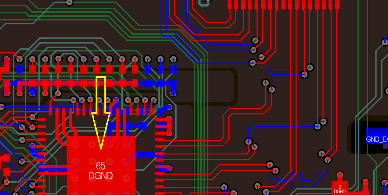
RF Trace PCB: Design Guidelines for Controlled Impedance & High-Frequency Signal Integrity

What is an RF Trace PCB? An RF Trace PCB refers to a printed circuit board specifically designed with controlled impedance traces to handle radio frequency (RF) signals. Unlike standard PCB routing, RF traces must maintain consistent electrical characteristics to avoid signal loss, reflection, and distortion. In RF design, the trace itself becomes part of...

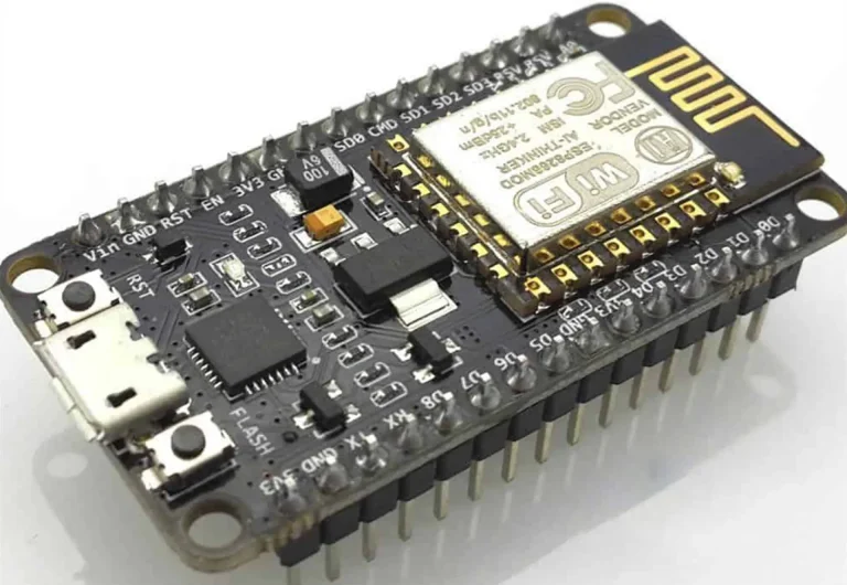
WiFi PCB Design Guide for High-Speed Connectivity: Architecture, Materials, RF Layout, and Best Practices

WiFi PCB Design Guide for High-Speed Connectivity Introduction WiFi connectivity is everywhere—from mobile devices to smart home systems and industrial machinery. At the heart of all these wireless systems lies the WiFi PCB, a specialized circuit board engineered to process, transmit, and receive high-frequency wireless signals. This guide explores the structure, design principles, materials, RF...

The Ultimate Guide to Bluetooth Modules and Bluetooth PCB Design: Architecture, RF Engineering, and Manufacturing Insights

What You Should Know About Bluetooth Modules and Bluetooth PCBs Bluetooth technology has become a cornerstone of short-range wireless communication, empowering devices such as headphones, speakers, smart appliances, wearables, industrial sensors, medical instruments, and countless IoT systems. At the heart of these wireless products lies a sophisticated combination of Bluetooth modules and Bluetooth PCBs, which...