HomeCategory

Advanced Engineering Technologies for PCB & PCBA Solutions - KKPCB

RF Via Transitions in High-Speed Designs: Best Practices and Considerations

In high-speed and RF PCB designs, controlling trace impedance is critical, but the role of RF via transitions is often underestimated. Vias, which connect signals between layers, can introduce impedance mismatches, signal reflections, and losses, especially at high frequencies. Proper design and optimization of via transitions are essential to maintain signal integrity and ensure reliable performance in RF and...
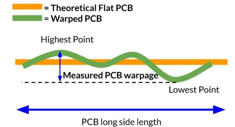
How to Check for PCB Warpage: Techniques and Methods

How to Check for PCB Warpage: Techniques and Methods PCB warpage (also known as bow and twist) is a common manufacturing defect that occurs when a printed circuit board deviates from perfect flatness. It can lead to serious issues during SMT assembly, such as poor solder joint formation, component misalignment, open circuits, or bridging. In...

Advanced PCB Footprint Generator: Key to Efficient PCB Design

1. Introduction: Why PCB Footprint Accuracy Matters in Modern Electronics In modern PCB design and electronic product development, accuracy at the earliest design stage directly determines manufacturing success, cost efficiency, and product reliability. One of the most critical elements in PCB layout design is the PCB footprint, which defines the physical land pattern for electronic...

Exploring the Current Carrying Capacity of Flexible PCBs

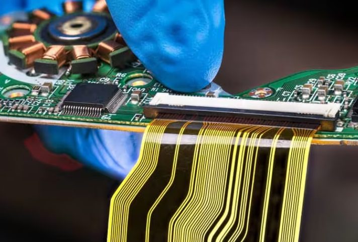
Understanding Current Capacity in Flexible PCBs Flexible PCBs (FPCs), typically manufactured with polyimide-based materials, are widely used in applications requiring compact size, lightweight construction, and dynamic bending capability. Compared with traditional rigid FR-4 PCBs, flexible circuits provide excellent mechanical flexibility and thermal resistance, making them suitable for automotive electronics, medical devices, wearable systems, industrial equipment,...

Optimizing PCB Trace Thickness vs. Current Capacity

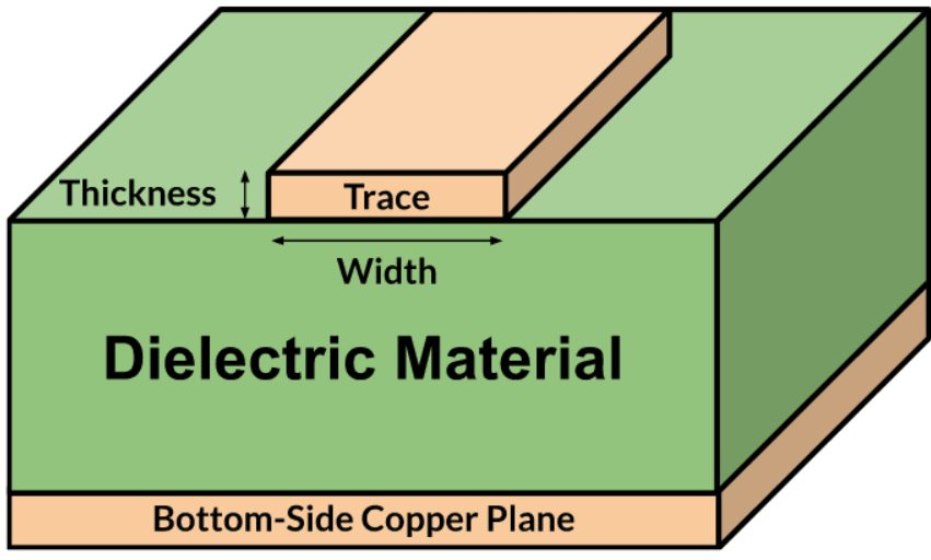
In PCB design, trace thickness and current carrying capacity are closely related factors that directly affect the reliability and performance of electronic systems. As electronic products continue moving toward higher power density, smaller form factors, and increased functionality, PCB traces must handle higher currents while maintaining acceptable temperature rise and electrical stability. Insufficient copper thickness...

PCB Routing: Best Practices for Ensuring Signal Integrity and Performance

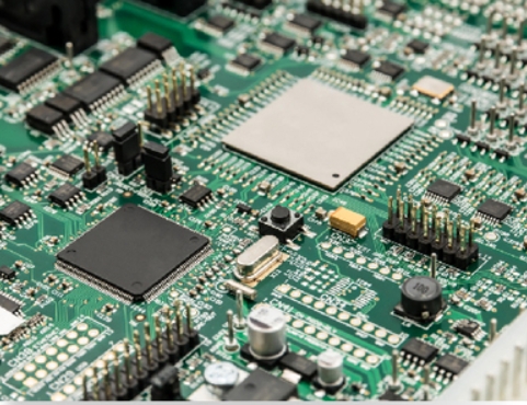
Printed Circuit Board (PCB) routing is a critical aspect of electronic design, ensuring that electrical signals are transmitted efficiently and reliably between components. Proper routing minimizes interference, maintains signal integrity, and meets design requirements such as impedance control and thermal management. This article outlines the best practices for PCB routing, focusing on optimizing performance and ensuring signal integrity....

Sensors and Transducers in Your PCB Design

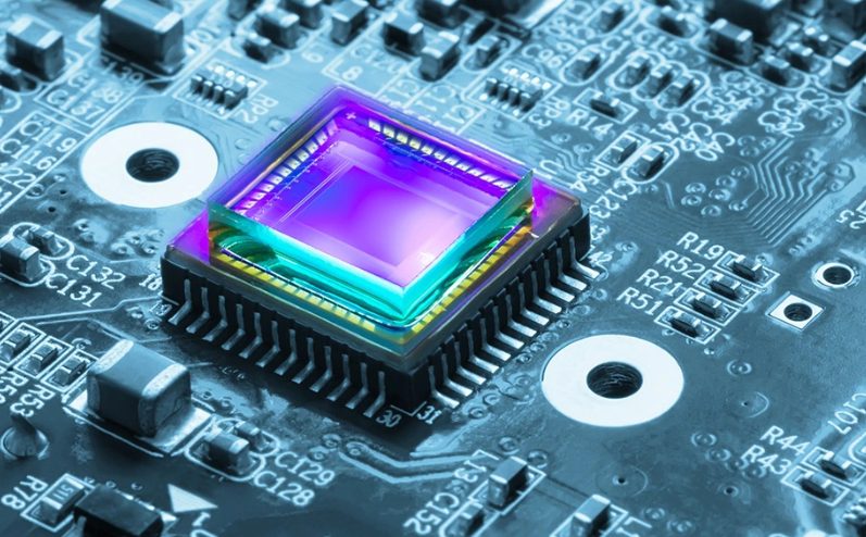
With the rapid development of industrial automation, IoT devices, smart manufacturing, medical electronics, and intelligent monitoring systems, sensors and transducers have become essential components in modern electronic products. A sensor detects physical parameters from the surrounding environment, while a transducer converts these physical signals into electrical signals that can be processed by electronic circuits. In...

The Most Common Manual PCB Soldering Defects

Why Manual PCB Soldering Quality Matters Although automated SMT PCB assembly is widely used in modern electronics manufacturing, manual PCB soldering remains essential for: Prototype PCB assembly Through-hole PCB assembly (THT) PCB rework and repair Low-volume electronics manufacturing Industrial and aerospace electronics maintenance However, improper manual soldering techniques can easily create PCB soldering defects, affecting:...

Ball Grid Array Technology Overview

What Is Ball Grid Array (BGA) Technology? Ball Grid Array (BGA) is an advanced surface mount packaging technology widely used in modern electronic products requiring high pin counts, high-speed signal transmission, and compact PCB layouts. Unlike traditional leaded packages, BGA components use an array of solder balls located underneath the package to create electrical and...

Can Pull-up Resistors Be Used on SPI Lines?

The SPI (Serial Peripheral Interface) is a widely used synchronous communication protocol in embedded systems, commonly applied for communication between: Microcontrollers (MCUs) Sensors Memory devices ADC/DAC converters Display controllers Communication modules Unlike protocols such as I²C, which use open-drain signaling and require pull-up resistors by design, SPI typically uses push-pull drivers. This leads to a...