Blog

Explore the KKPCB Blog for the latest PCB manufacturing and assembly news, industry insights, expert tips, and technology trends, helping you stay informed and optimize your electronics projects.
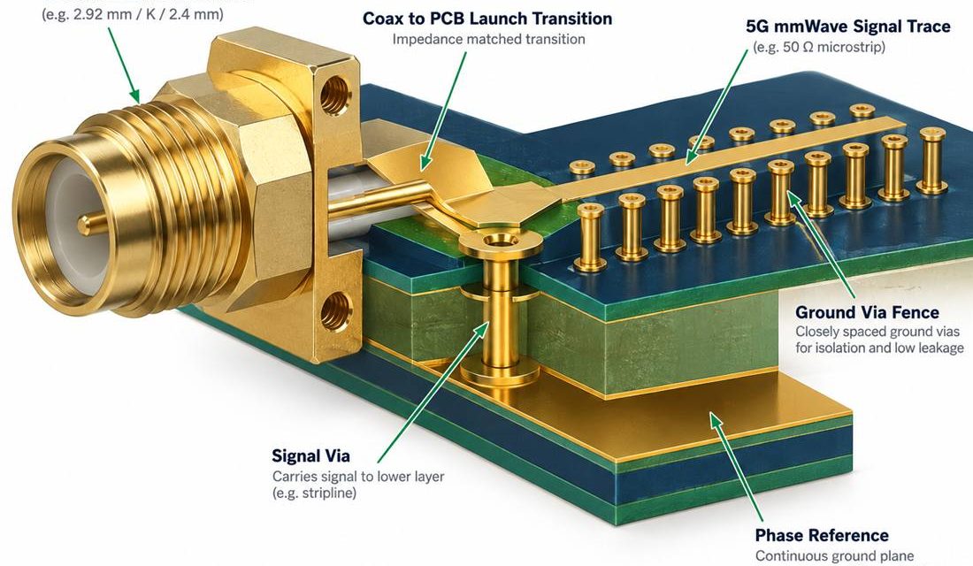
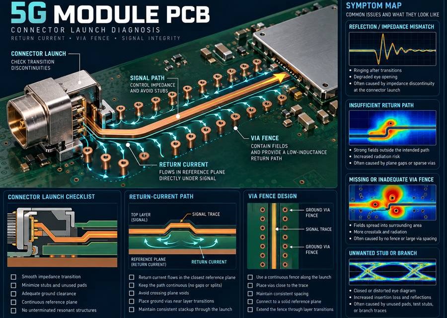
Designing Connector and Via Transitions for a 5G Module PCB Launch

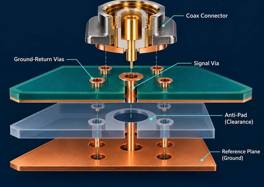
5G module PCB launch design begins with a complete three-dimensional signal and return path. The boundary between a board and a connector, coax, antenna, or shield is where a clean schematic becomes a three-dimensional electromagnetic problem. In compact radio modules used in private 5G radios, fixed-wireless units, and edge gateways, that boundary can set the...
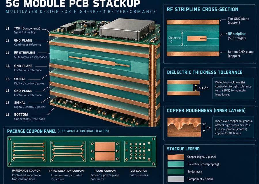
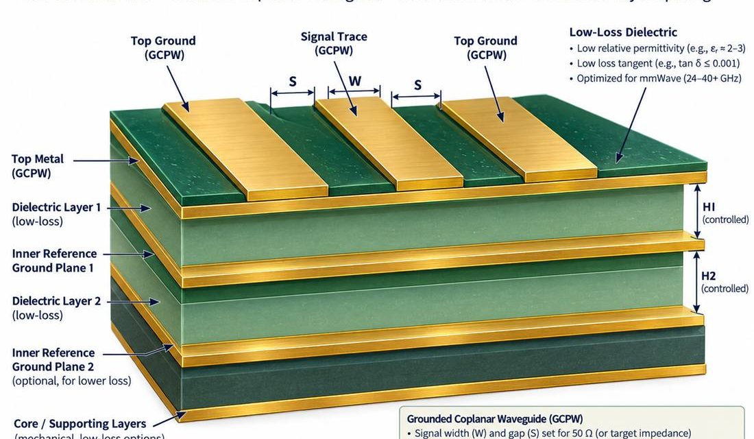
Selecting a 5G Module PCB Stackup Without Hiding the Loss Budget

5G module PCB stackup release begins by making every electromagnetic and manufacturing assumption visible. Stackup discussions fail when the drawing lists layer names but not the electromagnetic and manufacturing assumptions behind them. In compact radio modules used in private 5G radios, fixed-wireless units, and edge gateways, the board must carry RF energy, power current, high-speed...

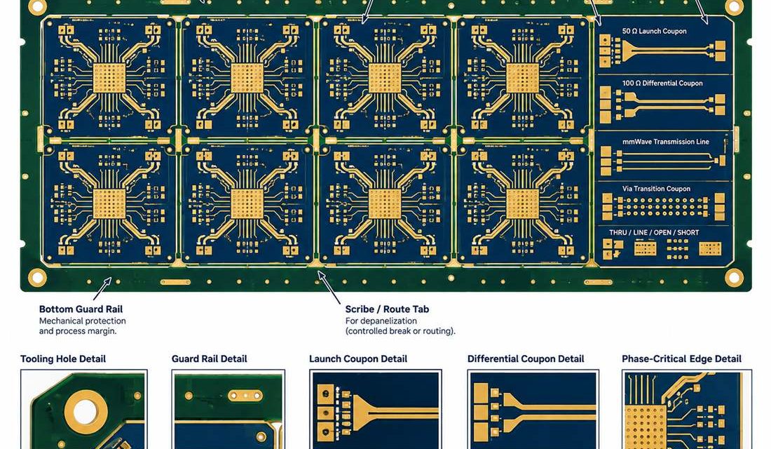
5G mmWave PCB DFM Release: 5 Production Checks

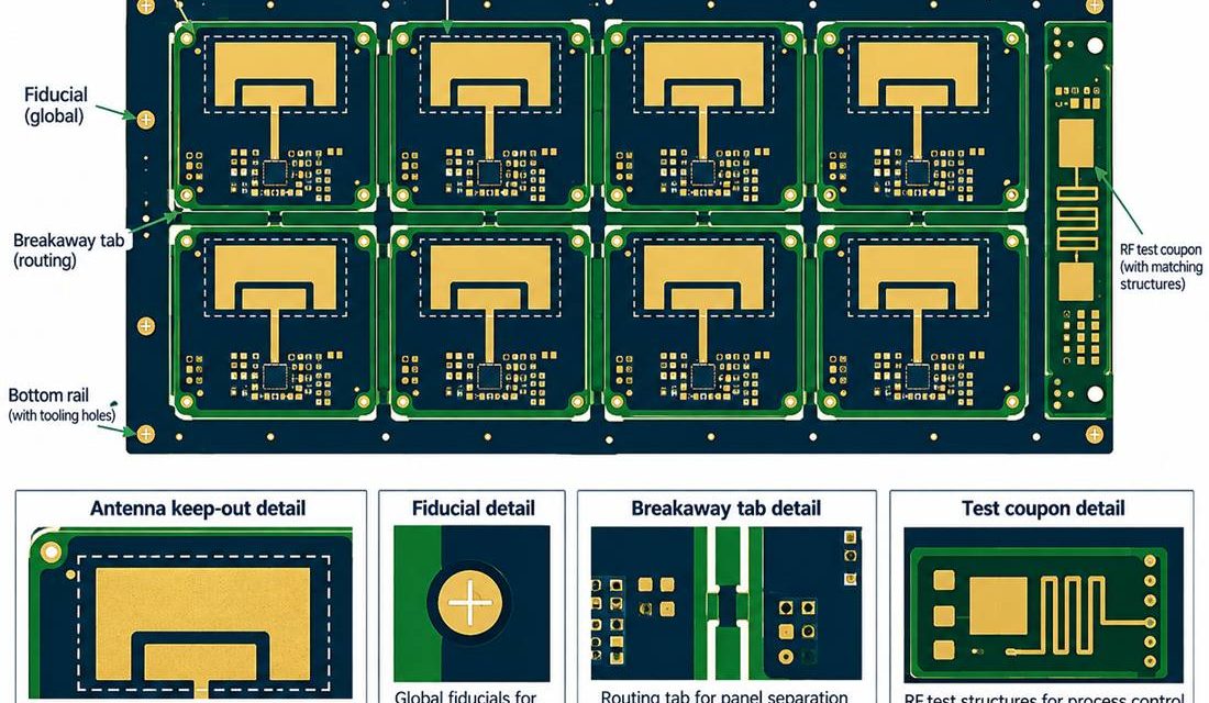
When a team selects 5G mmWave PCB, it is usually solving a specific product constraint rather than buying a label. This article takes a dfm view of millimetre-wave dielectric selection, connector launch geometry, via fences, and phase-matched RF channels. The project pain is a small mechanical offset or ground discontinuity becoming a larger phase, isolation,...

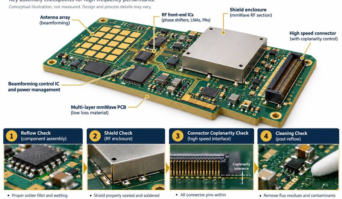
5G mmWave PCB Assembly: 5 Reliability Controls

When a team selects 5G mmWave PCB, it is usually solving a specific product constraint rather than buying a label. This article takes a assembly view of millimetre-wave dielectric selection, connector launch geometry, via fences, and phase-matched RF channels. The project pain is a small mechanical offset or ground discontinuity becoming a larger phase, isolation,...

5G mmWave PCB Via Launch: 5 Transition Checks

When a team selects 5G mmWave PCB, it is usually solving a specific product constraint rather than buying a label. This article takes a transition view of millimetre-wave dielectric selection, connector launch geometry, via fences, and phase-matched RF channels. The project pain is a small mechanical offset or ground discontinuity becoming a larger phase, isolati...

5G mmWave PCB Stack-Up: 5 Geometry Controls

When a team selects 5G mmWave PCB, it is usually solving a specific product constraint rather than buying a label. This article takes a stackup view of millimetre-wave dielectric selection, connector launch geometry, via fences, and phase-matched RF channels. The project pain is a small mechanical offset or ground discontinuity becoming a larger phase, isolation,...

5G mmWave PCB Thermal Path: 5 Release Checks

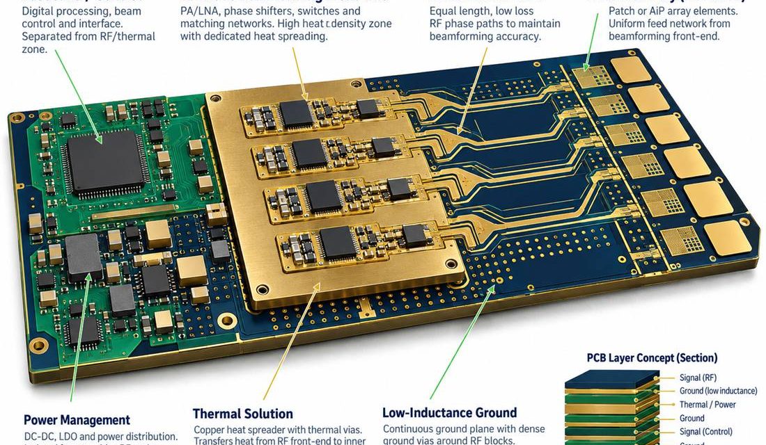
When a team selects 5G mmWave PCB, it is usually solving a specific product constraint rather than buying a label. This article takes a thermal view of millimetre-wave dielectric selection, connector launch geometry, via fences, and phase-matched RF channels. The project pain is a small mechanical offset or ground discontinuity becoming a larger phase, isolation,...

5G antenna PCB DFM Release: 5 Production Checks

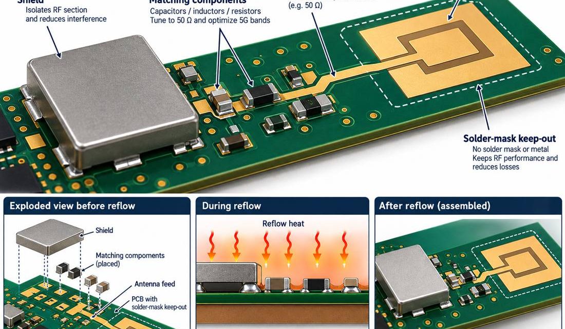
When a team selects 5G antenna PCB, it is usually solving a specific product constraint rather than buying a label. This article takes a dfm view of antenna aperture geometry, feed transitions, matching features, enclosure clearance, and reference-plane control. The project pain is a feed that is nominally 50 ohms but is detuned by housing...

5G antenna PCB Assembly: 5 Reliability Controls

When a team selects 5G antenna PCB, it is usually solving a specific product constraint rather than buying a label. This article takes a assembly view of antenna aperture geometry, feed transitions, matching features, enclosure clearance, and reference-plane control. The project pain is a feed that is nominally 50 ohms but is detuned by housing...