
HomeTag

PCB Design - KKPCB

About PCB Layer Stackup

A PCB Layer Stackup refers to the arrangement of conductive copper layers and insulating dielectric materials that make up a multilayer PCB. In the era of high-speed digital electronics and 5G, the stackup is no longer just a mechanical carrier; it is a critical tool for managing signal integrity, power distribution, and electromagnetic compatibility (EMC). A well-engineered stackup from KKPCB ensures...
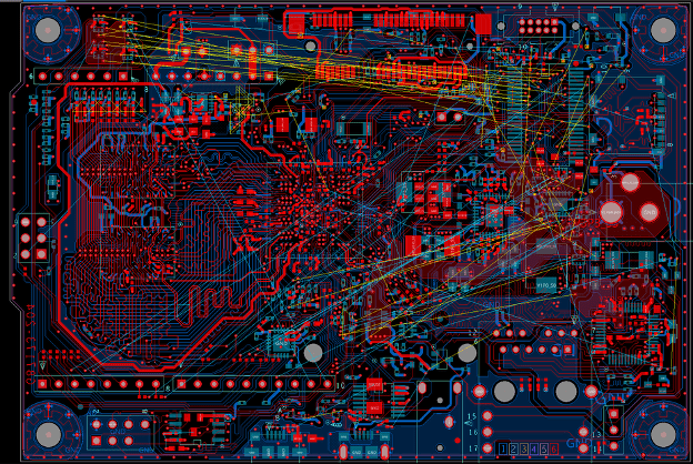
Basic Knowledge You Need to Master for PCB Design

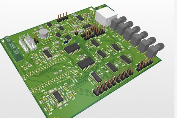
PCB (Printed Circuit Board) design is a fundamental process in electronic product development. A well-designed PCB not only provides electrical connections between components but also directly affects: Signal integrity Power stability Electromagnetic compatibility (EMC) Thermal performance Manufacturing reliability With the increasing complexity of modern electronic systems, PCB design is no longer limited to simple component...

Basic Principles and Operations of PCB Wiring

PCB wiring, also known as PCB routing, is one of the most critical stages in printed circuit board design. It determines how electrical signals and power are transmitted between components and directly affects the performance, reliability, and manufacturability of electronic products. With modern electronic systems moving toward higher speed, higher density, and greater integration, PCB...

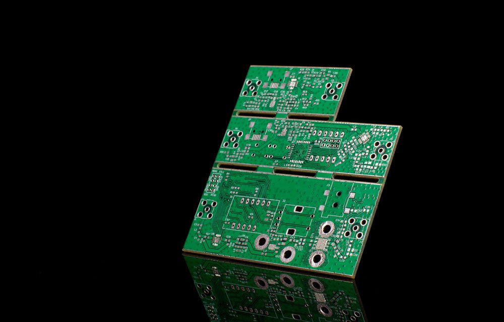
Blind Via and Buried Via

In modern PCB design, Blind Via and Buried Via technologies play a critical role in achieving high-density interconnect (HDI) structures, improving signal integrity, and optimizing PCB layout performance. As electronic devices continue to evolve toward miniaturization, high speed, and high functionality, the use of blind vias and buried vias has become increasingly essential in advanced...

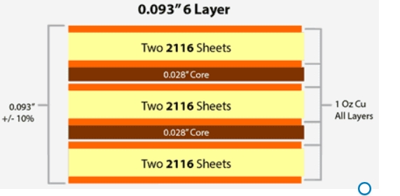
6 layer PCB Stackup,Thickness and Manufacturing

Printed circuit boards (PCBs) have evolved from simple single or double layer boards to complex multilayer boards with 6 or more layers to accommodate increasing component density and interconnectivity needs. 6 layer PCBs provide more flexibility for routing, plane separation and enable partitioning of circuits across layers. However, designing the 6 layer stackup requires careful planning to utilize...

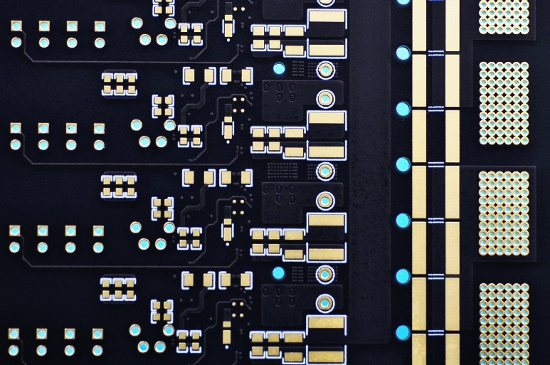
Annular Ring in PCB: Key Considerations for Design and Manufacturing

In PCB design and manufacturing, every detail of the circuit structure can influence the reliability and performance of the final product. Among these details, the annular ring is a critical but often overlooked factor that directly affects via reliability, electrical connectivity, and manufacturing yield. The annular ring refers to the copper area surrounding a drilled...

Rigid-Flex PCBs: Features, Benefits and Challenges

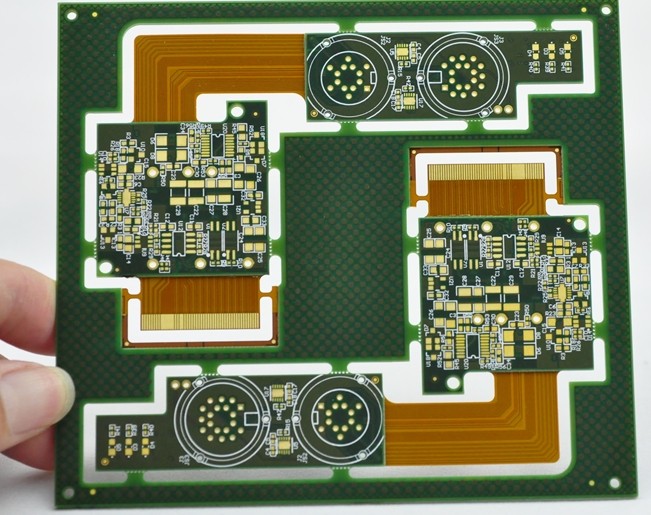
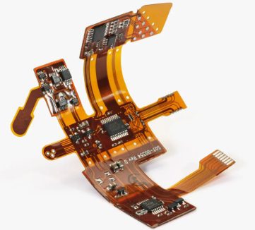
Introduction: The Rise of Rigid-Flex PCB Technology As modern electronics continue to evolve toward miniaturization, high reliability, and complex system integration, Rigid-Flex PCBs have become a key solution in advanced PCB design and manufacturing. By combining the strengths of rigid PCBs and flexible PCBs, Rigid-Flex PCB technology enables innovative product designs that are both compact...

Rigid-Flex PCB Cost Optimization: Design and Manufacturing Considerations

As the demand for flexible and rigid-flex PCBs continues to grow, understanding the factors that influence their cost is crucial for optimizing designs and ensuring cost-effective production. Rigid-flex PCBs offer significant advantages, such as enhanced flexibility, reliability, and space-saving capabilities, but they also come with unique challenges that can drive up costs if not properly managed. This...

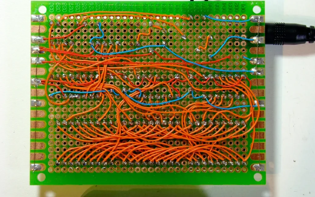
PCB Drawing: A Summary of Key Practices from Years of Experience

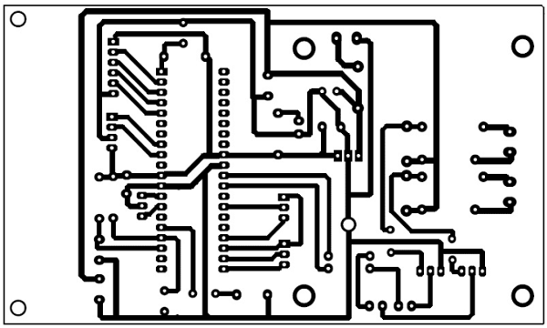
PCB drawing is a critical stage in electronic product development that transforms circuit concepts and schematic designs into physical circuit boards. Although modern PCB design software has significantly improved design efficiency, creating a reliable PCB drawing still requires extensive engineering experience. A PCB layout must not only achieve electrical connections but also consider signal integrity,...

Complete Guide to ESD Prevention in PCB Design

Electrostatic discharge (ESD) is one of the most common reliability challenges in modern electronic products. With increasing levels of integration, smaller component packages, and faster signal transmission speeds, electronic devices have become more sensitive to transient electrical disturbances. ESD events can occur during: Product assembly Transportation User operation Maintenance activities External cable connection A sudden...