
PCB wiring, also known as PCB routing, is one of the most critical stages in printed circuit board design. It determines how electrical signals and power are transmitted between components and directly affects the performance, reliability, and manufacturability of electronic products.
With modern electronic systems moving toward higher speed, higher density, and greater integration, PCB wiring is no longer simply a process of connecting components. Engineers must consider multiple factors, including:
- Signal integrity
- Power integrity
- Electromagnetic compatibility (EMC)
- Thermal performance
- Manufacturing capability
A well-designed PCB wiring structure can reduce signal interference, improve system stability, and ensure smoother transition from prototype development to mass production.
1. What Is PCB Wiring?
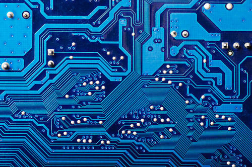
PCB wiring refers to the process of creating copper traces on a PCB layout to electrically connect components according to the schematic design.
The main purpose of PCB wiring is to establish reliable electrical paths for:
- Signal transmission
- Power delivery
- Ground return paths
PCB wiring includes several key elements:
- Trace width
- Trace spacing
- Routing direction
- Via structures
- Layer assignment
- Grounding methods
The quality of wiring directly affects electrical performance and manufacturing reliability.
2. Basic PCB Wiring Process
2.1 Review the Schematic and Design Requirements
Before starting PCB wiring, engineers should fully understand the circuit structure.
Important information includes:
- Signal flow
- Power requirements
- Component functions
- Critical signal paths
- Interface requirements
A clear understanding of the schematic helps establish a reasonable routing strategy.
2.2 Define PCB Stack-Up
For multilayer PCBs, stack-up design should be determined before routing.
The stack-up affects:
- Signal impedance
- Return current paths
- EMI performance
- Thermal behavior
Typical multilayer structures include:
- Signal layers
- Ground planes
- Power planes
- Mixed signal layers
A properly designed stack-up provides a stable foundation for PCB wiring.
2.3 Component Placement Optimization
Good PCB wiring starts with proper component placement.
Key principles include:
Functional Separation
Components should be grouped according to their functions:
- Power circuits
- Analog circuits
- Digital circuits
- RF circuits
This reduces interference between different circuit sections.
Short Signal Paths
Critical components should be placed close together to minimize:
- Signal delay
- Transmission loss
- Noise coupling
Thermal Considerations
Heat-generating components should be positioned with proper thermal paths.
Examples include:
- Power ICs
- Voltage regulators
- Drivers
3. Basic Principles of PCB Wiring
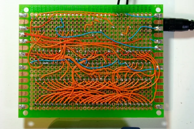
3.1 Follow the Shortest and Most Direct Routing Path
Short routing paths reduce:
- Signal delay
- Resistance
- Electromagnetic radiation
For high-speed signals, unnecessary routing length should be avoided.
3.2 Maintain Appropriate Trace Width
Trace width affects:
- Current carrying capability
- Voltage drop
- Heat generation
Power traces generally require wider widths than signal traces.
Design considerations include:
- Current requirements
- Copper thickness
- Temperature rise limitations
3.3 Maintain Proper Trace Spacing
Adequate spacing helps prevent:
- Signal interference
- Electrical shorts
- Crosstalk
Spacing requirements depend on:
- Voltage level
- Signal frequency
- Manufacturing capability
3.4 Consider Signal Return Paths
Every signal requires a return current path.
A poor return path may cause:
- Increased noise
- EMI problems
- Signal distortion
Good practices include:
- Maintaining continuous reference planes
- Avoiding unnecessary plane gaps
- Minimizing return path changes
4. High-Speed Signal Routing Principles
High-speed PCB wiring requires additional design considerations.
4.1 Controlled Impedance Design
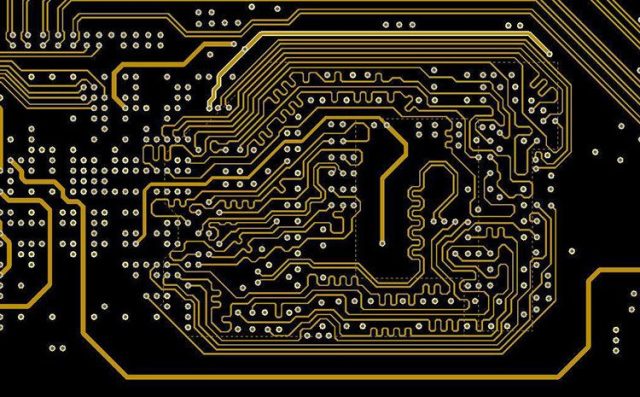
High-speed signals are sensitive to impedance variation.
Engineers should control:
- Trace width
- Dielectric thickness
- Copper thickness
- Reference plane distance
Common controlled impedance structures include:
- Microstrip
- Stripline
- Differential pair routing
4.2 Differential Pair Routing
Differential signals require:
- Consistent spacing
- Matched trace lengths
- Symmetrical routing
Applications include:
- USB
- Ethernet
- PCIe
- High-speed communication interfaces
4.3 Length Matching
For timing-sensitive signals, trace length matching is required.
Common applications:
- Memory interfaces
- High-speed data buses
- Clock networks
Proper length matching reduces timing errors.
5. Power and Ground Wiring Principles
5.1 Power Distribution Design
Power routing should consider:
- Current flow
- Voltage stability
- Noise control
Recommended methods include:
- Wider power traces
- Dedicated power planes
- Proper capacitor placement
5.2 Ground Design
Grounding is one of the most important PCB design factors.
Good grounding practices include:
- Using complete ground planes
- Reducing ground loops
- Separating noisy and sensitive areas when necessary
Poor grounding may cause:
- Signal instability
- EMI issues
- System malfunction
6. PCB Wiring for EMC and EMI Control
Electromagnetic compatibility should be considered during routing.
6.1 Reduce High-Frequency Current Loops
Smaller current loops help reduce electromagnetic radiation.
Important areas include:
- Switching power supplies
- Clock circuits
- RF circuits
6.2 Separate Sensitive and Noisy Circuits
High-noise circuits include:
- Motor drivers
- Switching regulators
- High-current circuits
Sensitive circuits include:
- Sensors
- Analog amplifiers
- Communication receivers
Proper separation reduces interference.
6.3 Use Grounding and Shielding Techniques
Methods include:
- Ground planes
- Ground vias
- Shielding structures
These improve EMC performance.
7. PCB Wiring Considerations for Manufacturing
PCB wiring must consider manufacturing requirements.
7.1 Design Rule Check (DRC)
Before fabrication, engineers should verify:
- Trace spacing
- Minimum width
- Via rules
- Clearance requirements
7.2 Via Design
Vias provide electrical connections between PCB layers.
Important factors include:
- Hole size
- Pad diameter
- Annular ring
- Aspect ratio
Poor via design may reduce reliability.
7.3 Avoid Manufacturing Risks
Common issues include:
- Extremely narrow traces
- Insufficient spacing
- Excessive via density
- Uneven copper distribution
Early DFM review helps prevent these problems.
8. Common PCB Wiring Mistakes
8.1 Improper Ground Routing
Problems:
- Increased noise
- Poor signal stability
8.2 Excessive Trace Length
Problems:
- Signal delay
- Increased loss
8.3 Incorrect Power Routing
Problems:
- Voltage drop
- Thermal issues
8.4 Ignoring Manufacturing Capability
Problems:
- Low production yield
- Increased manufacturing cost
9. PCB Wiring Optimization Methods
Professional PCB wiring optimization includes:
Simulation Analysis
For advanced designs:
- Signal integrity simulation
- Power integrity analysis
- Thermal simulation
Engineering Review
A detailed review helps identify:
- Layout risks
- Manufacturing issues
- Reliability concerns
DFM Optimization
DFM analysis ensures that PCB wiring is compatible with production processes.
Conclusion
PCB wiring is a fundamental process that determines the electrical performance, reliability, and manufacturability of a circuit board.
Effective PCB wiring requires more than simply connecting components. Engineers must consider signal integrity, power distribution, grounding, EMI control, thermal management, and manufacturing requirements throughout the design process.
By following proper wiring principles and applying engineering optimization methods, designers can create PCB layouts with improved performance, higher reliability, and better production readiness.
