HomeTag

multilayer PCB - KKPCB

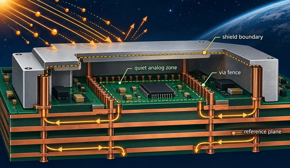
Satellite PCB Radiation Design for LEO Avionics: Dielectrics, Planes, and Shielded Returns

Satellite PCB radiation design for low-Earth-orbit avionics is often reviewed too late as a materials choice. The difficult question is not whether a board can route a signal; it is whether the dielectric, copper stack, enclosure bond, and return current still behave predictably after radiation exposure, thermal cycling, launch handling, and repeated engineering changes. A...
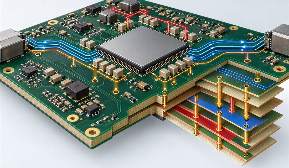
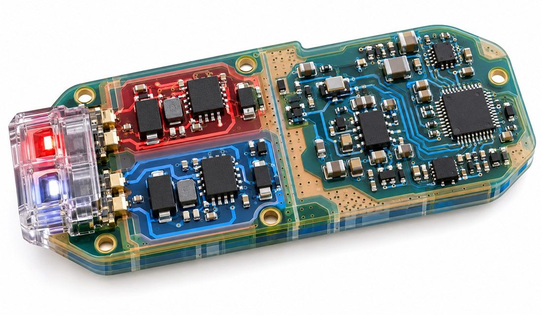
Aerospace PCB Design for FPGA Flight Computers: Stackup, PDN, and Return-Path Tradeoffs

Table of Contents Why a flight-computer board needs an SI/PI-first layout study Build the stackup around the package escape and power loop Translate FPGA load steps into a PDN verification plan Protect high-speed returns through connectors and board boundaries Make the mechanical and manufacturing boundary explicit Use release evidence that survives a late component or...

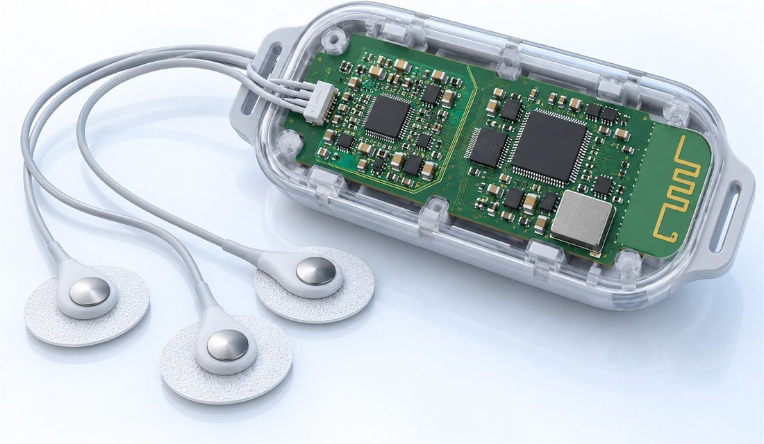
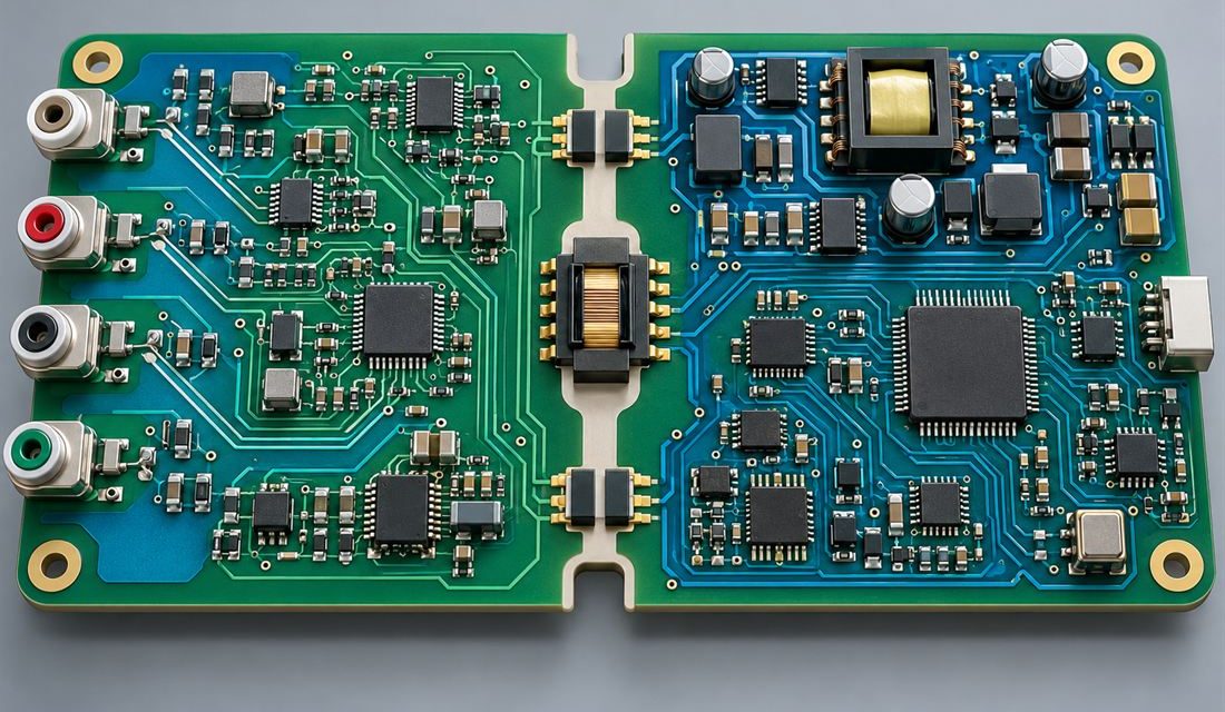
Healthcare PCB Isolation Boundaries: Plan Power and Data Separation in Patient Monitors

Healthcare PCB isolation for a patient monitor starts with a system boundary, not a board outline. A monitor can meet its functional targets in a bench setup and still fail a board-level review when the patient-connected signal domain, digital processor, and power conversion are treated as one undifferentiated ground system. On a Healthcare PCB, isolation...

When Ultrasound Echoes Become Layout Noise: A Low-Noise Ultrasound PCB Release Plan

Ultrasound PCB design fails in a very specific way: the image can look acceptable on a bench and then lose contrast when transmit voltage, receive gain, clock activity, and patient-interface cabling are present at the same time. The difficult part is not choosing an expensive AFE; it is preserving the receive signal while the board...

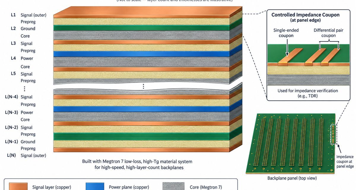
How to Freeze a Megtron 7 PCB Stackup When Layer Count and Impedance Must Move Together

A Megtron 7 PCB stackup must be frozen as an electrical and manufacturing contract before layer count or impedance changes are approved. High-layer-count digital boards rarely fail because an engineer forgot to draw a trace. They fail when a late layer move changes dielectric thickness, resin distribution, or reference-plane continuity and the impedance model is...

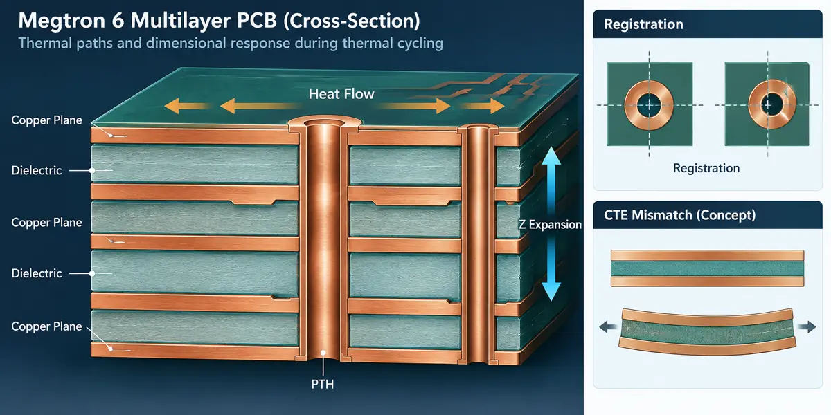
Megtron 6 PCB Thermal Cycling: Keeping Dense Multilayer Registration Predictable

The controlled Megtron 6 PCB datum should be reviewed before thermal cycling begins. For a dense compute Megtron 6 PCB, copper balance and registration targets belong in the same release package. A second Megtron 6 PCB construction should never be approved without a revised coupon plan. Megtron 6 PCB thermal reliability is a registration problem...

RO4003C PCB Stackup Release: Managing Dielectric Thickness in Compact RF Modules

Compact RF modules often fail between schematic approval and fabrication release because the RO4003C PCB stackup is treated as a static drawing. Resin content, copper thickness, press-out, and reference-plane choices change the field geometry that the RF model used. A controlled RO4003C PCB stackup release turns those assumptions into a buildable document for engineering and...