
An RF power board can pass an electrical review and still fail in the field when heat changes the laminate geometry, connector datum, or solder-joint stress. This engineering guide treats the RO4350B PCB as a thermal and RF structure for high-power modules. The values below are planning guidance based on vendor-typical material behavior and KKPCB public process categories, not measured customer results.
Start with the heat path, not only the trace width
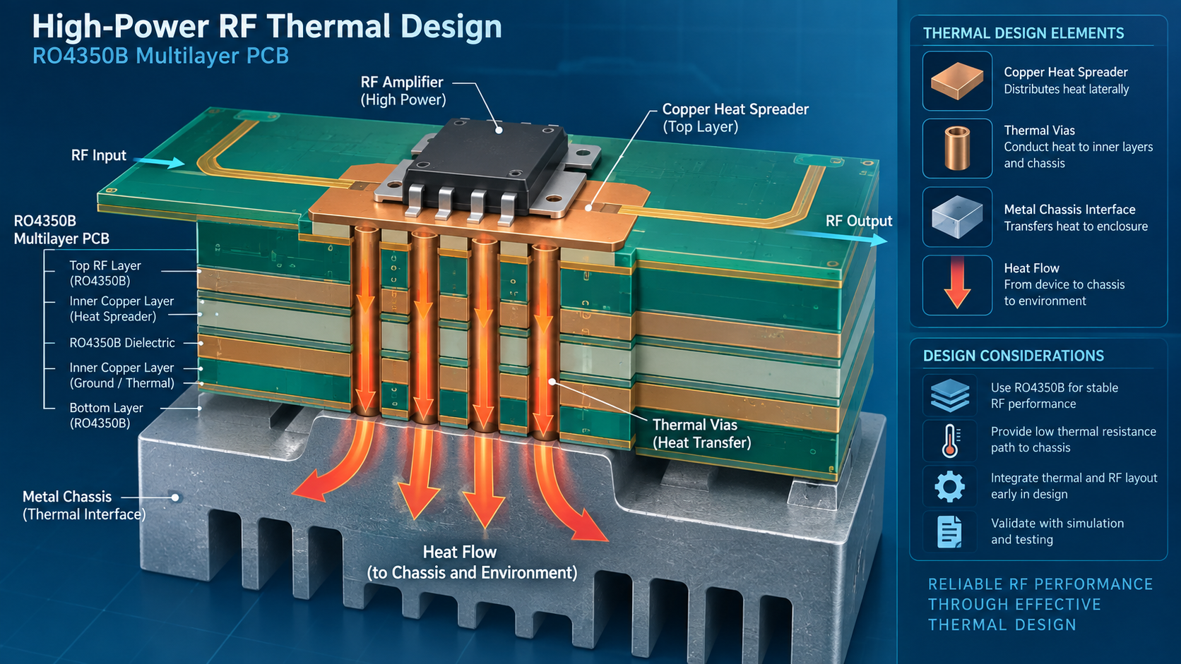
A high-power RO4350B PCB must move heat from the RF device into copper planes, thermal vias, the chassis interface, and finally the enclosure. A wide RF trace helps current density, but it does not replace a low-resistance thermal path. Mark the device pad, exposed ground, copper spreader, via field, and mechanical clamp on the first stackup review.
| Thermal decision | Typical failure mode | Engineering control |
|---|---|---|
| Heat source | Power amplifier pad is isolated from the plane. | Use a defined copper landing and a via field that the released drill class can produce. |
| Plane spreader | Thermal copper is segmented by RF clearances. | Reserve a continuous copper region and check the RF keep-out against the thermal target. |
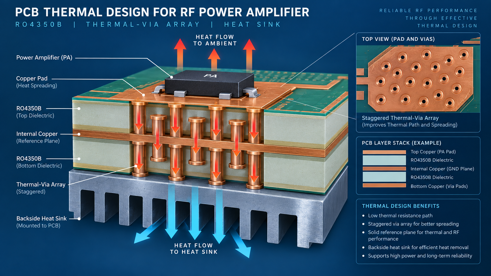
| Via array | Voids or resin starvation reduce heat transfer. | Specify filled or capped vias only when the approved process and inspection support it. |
| Chassis path | Board-to-enclosure contact adds an unplanned thermal interface. | Define flatness, interface material, screw pattern, and compression ownership. |
Choose copper geometry with RF and thermal constraints together
The RO4350B PCB stackup should identify which copper layers spread heat and which layers remain quiet RF references. Heavy copper can reduce DC loss, but abrupt copper transitions can change impedance and etch behavior. Keep the device launch, ground return, and thermal spreader aligned instead of adding isolated copper islands.
For a multilayer PCB, review copper balance across the panel. A large copper pour on one side and a sparse return on the other can increase bow, twist, and registration risk. Use symmetric constructions where the design allows, and let the fabricator confirm resin fill, finished dielectric, and copper profile before locking the RF model.
Thermal-via array rules
Thermal vias should connect the device pad to the intended reference plane without cutting through an adjacent launch antipad. Keep the array boundary away from controlled RF neck-downs and connector transitions. The correct pitch depends on drill diameter, pad size, plane clearance, and heat load; do not publish a universal spacing as if it were a guaranteed KKPCB value.
Manage material and mechanical expansion
Rogers RO4350B material data provide vendor-typical dielectric and thermal context. Finished dielectric thickness, copper roughness, resin flow, and local copper density still depend on the released construction. Any PCB materials substitution should trigger a new impedance and thermal review, especially when the RF path is close to a heat spreader.
Mechanical design matters at the same time. A board-edge connector, screw, or stiffener can move the local neutral axis and concentrate stress near a hot component. Keep the thermal-via field clear of unsupported slots, mounting holes, and routed depanelization features. A PCB manufacturing drawing should show the datum, copper-to-edge clearance, mask opening, and any controlled-depth routing.
Use a qualification plan that separates targets from evidence
An engineering team may set a junction-temperature target, a board temperature limit, and an allowable impedance shift. These are design targets, not measured KKPCB results. Record the material source, stackup revision, power waveform, fixture, thermocouple location, and ambient condition before calling a result qualified.
- Define the power device, duty cycle, and heat-source footprint.
- Review the copper spreader and thermal-via field with RF clearances visible.
- Confirm finished dielectric, copper balance, and surface finish with the fabricator.
- Run a thermal model or bench test only when the method and data owner are documented.
- Close any deviation through a controlled ECO before production release.
Project handoff checklist
- The RO4350B PCB release names the heat source, reference plane, and chassis interface.
- Thermal vias, pad finish, and inspection limits are shown on the fabrication drawing.
- The HDI PCB escape does not cut the RF return or thermal plane unexpectedly.
- Material substitutions receive a renewed impedance and thermal sign-off.
- The PCB manufacturing team owns panel, bow, twist, and via-quality acceptance.
Questions engineers ask
Does thicker copper always reduce RF temperature?
No. It can lower resistive loss, but copper distribution, via resistance, interface contact, and airflow also control temperature.
Should thermal vias be filled on every board?
No. Filling is a process decision tied to pad geometry, soldering, reliability, and inspection capability.
Can a material change be approved from the nominal Dk alone?
No. Recheck finished thickness, copper profile, resin behavior, loss, and the thermal path together.
Sources: Rogers RO4350B manufacturer data provide vendor-typical material context; KKPCB public High-Frequency PCB, PCB Materials, HDI PCB, Multilayer PCB, and PCB Manufacturing pages verify service categories. No external hyperlinks or claimed customer measurements are used.
Thermal sign-off for the RO4350B PCB
Assign one owner to the RF launch, one to thermal validation, and one to fabrication acceptance. The RO4350B PCB package should carry the same revision across the stackup, thermal drawing, assembly notes, and test fixture. If the enclosure or power device changes, reopen the thermal-via, copper-balance, and impedance review before panel release.
For final release, the RO4350B PCB thermal path and the RO4350B PCB material revision must be checked together. Keep the RO4350B PCB stackup, RO4350B PCB via field, RO4350B PCB copper spreader, and RO4350B PCB enclosure interface on the same revision checklist.
