
When designing an Aerospace PCB around an FPGA flight computer for a compact avionics card, routing congestion is often the first visible problem. The harder failure mode is that the board was partitioned before the power-distribution network (PDN), high-speed interfaces, package escape, and mechanical envelope were treated as one design problem. A trace can pass a layout check and still lose its return path at a layer transition; a decoupling network can look adequate at the schematic stage and then miss the processor’s transient-current demand after the stackup is fixed.
This guide is for teams releasing a new Aerospace PCB around an FPGA or high-performance processor. It turns those coupled constraints into a sequence of decisions that a board designer, power engineer, mechanical engineer, and project lead can review together—before an expensive integrated build becomes the first useful test.
Why a flight-computer board needs an SI/PI-first layout study
Space electronics teams often have to balance processing throughput, power, volume, mission duration, component assurance, and cost. NASA’s published work on the SpaceCube v3.0 Mini is a useful engineering reference because it treats signal integrity and power integrity as part of processor-board architecture, not as a late cleanup step. The study describes how smaller form factors and dense FPGA/processor designs raise the difficulty of power distribution, transient response, and routing. Its reported impedance and capacitor tradeoffs apply to that specific design and mission analysis; they are not default targets for another board.
The practical lesson is to define the interface and power problem before fixing the outline. Start with the FPGA package, memory and transceiver interfaces, clock sources, voltage rails, connector locations, estimated load steps, heat-removal path, mounting points, and allowed board thickness. Rank interfaces by data rate, edge behavior, sensitivity, length matching, and consequence of failure. The resulting priority list helps an engineer allocate routing layers and reference planes instead of trying to rescue every net after placement.
A short early PCB layout study should include component placement without detailed routing, a preliminary breakout assessment, and a first-pass mechanical envelope. NASA’s spacecraft board-layout guidance specifically recommends early density studies and collaboration with mechanical design on outline, thermal interfaces, and stackup thickness. For a program manager, this is a schedule-control step: it makes connector, package, and layer-count conflicts visible while component or outline changes are still relatively inexpensive.
Build the stackup around the package escape and power loop
Do not select a layer count just because a previous avionics card used it. The stackup must accommodate BGA escape, controlled-impedance routes, continuous reference planes, the PDN, via transitions, copper balance, and the fabricator’s actual drill and lamination constraints. A package with tight pitch may require more escape capacity; that does not automatically mean that every signal should be pushed into a microvia structure. Compare the benefit of HDI interconnect against added sequential lamination, via reliability, and cost before locking the design.
Keep critical signal layers adjacent to an uninterrupted reference plane wherever possible. If a route changes layers, provide a nearby ground transition so return current can move with the signal instead of finding a distant path around plane splits or antipads. Reserve a low-inductance local loop for the processor power pins: package escape vias, plane connection, capacitor location, and the capacitor mounting inductance all matter. The board is not just a set of isolated trace-width calculations; geometry and current loops interact across the assembled structure.
For an Aerospace PCB, coordinate the preliminary stackup with a manufacturing engineer before routing is mature. Dielectric thickness, copper weights, finished thickness, via aspect ratio, registration, and impedance coupons must be considered together. KKPCB’s public PCB manufacturing capabilities list is a useful starting point for a capability discussion, not a substitute for approving the exact construction and acceptance plan for a specific flight program. Record the agreed materials, layer sequence, finished copper, tolerances, and coupon requirements in a controlled construction drawing.
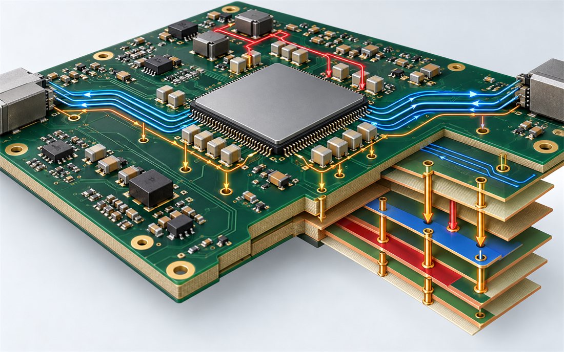
Translate FPGA load steps into a PDN verification plan
Average current is not enough to size a processor rail. Collect each rail’s nominal voltage, tolerance allocation, DC regulator accuracy, expected current range, load-step magnitude and edge, decoupling constraints, and temperature conditions. Then derive a target impedance from the actual voltage budget and transient requirement. Treat it as a design constraint for the relevant frequency range, not a single magic number copied from another project.
NASA’s flight-computing study illustrates why the tolerance budget matters: regulator accuracy, temperature, load regulation, radiation-related part variation, and transient behavior can change the margin available to the PDN. Its example calculation and SpaceCube-specific result are evidence that the budget should be mission-aware, not universal. For a new design, run both frequency-domain impedance analysis and time-domain load-step checks with the chosen stackup, via fields, capacitor models, and component placement. Check whether a seemingly small change—moving a capacitor, changing plane spacing, or swapping a regulator—pushes a resonance or worsens the local loop.
Keep the power engineer involved through placement and routing. A low-impedance plane pair can help, but plane area alone does not guarantee a good response if the package breakout, anti-pad pattern, or capacitor mounting inductance dominates. Tie each simulated or calculated criterion to its assumptions and revision. If a value is a preliminary engineering target, label it as such; do not present it later as a measured board result. When choosing a low-loss route for a clock or RF interface, evaluate the material and geometry in the context of the complete high-frequency PCB construction, not just a laminate datasheet number.
Protect high-speed returns through connectors and board boundaries
On an Aerospace PCB, high-speed signals usually leave the FPGA through a connector, mezzanine, or backplane. That transition is a system interface, not merely a footprint. Confirm connector pin assignment, adjacent ground contacts, escape routing, via stub strategy, chassis bonding, and the return path on both sides of the interface. If the connector is mounted at a board edge, include the card guide, stiffener, fasteners, enclosure ground, and mating-board tolerance in the same review. A connector launch optimized in isolation can be undermined by a ground discontinuity or a mechanical keep-out that forces the return current to detour.
For each critical differential or single-ended interface, document the source and load, reference layer, permitted routing corridor, transition count, length or skew requirement, and the method used to verify it. Use vendor package models and connector data when available; if they are unavailable, identify the limitation and keep the design margin explicit. Do not claim a validated eye, insertion loss, or radiation performance without a defined model or actual measurement. A structured prototype assembly can be used to learn about assembly access and bring-up sequencing, but an engineering prototype is not flight qualification.
Keep a clear ground-reference corridor under critical paths and inspect every layer transition in cross-section. For interfaces that must cross a plane gap, add a deliberate return bridge or move the crossing; do not rely on a distant chassis connection to repair a local discontinuity. The Aerospace PCB material and routing discussion should include copper roughness, dielectric loss, and tolerance only when the interface’s edge rate and length make them decision-relevant.
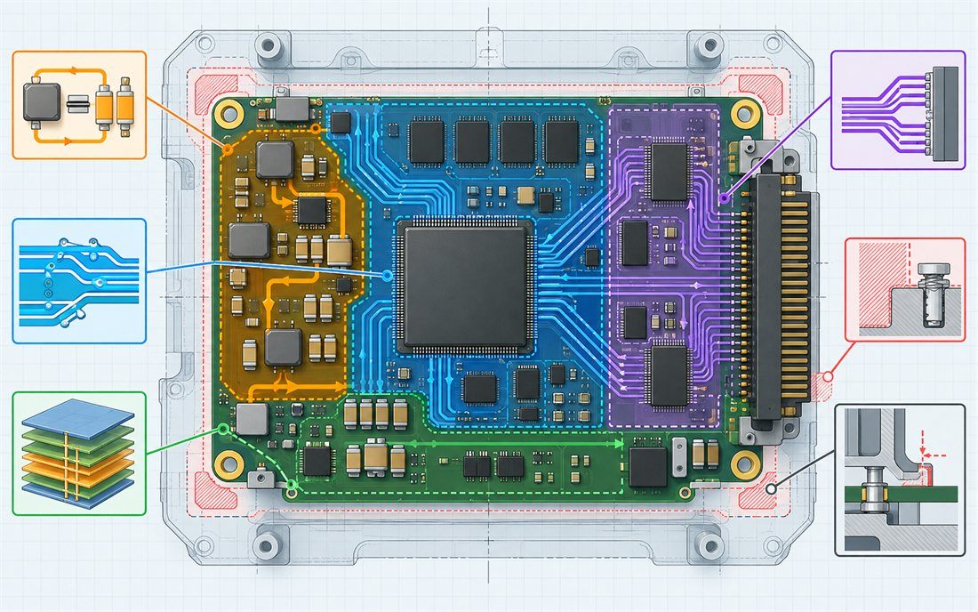
Make the mechanical and manufacturing boundary explicit
In an Aerospace PCB, board thickness, support points, connector insertion force, component mass, fastener torque, and thermal contact are coupled to copper and laminate choices. If an enclosure or cold plate contacts the board, identify the intended heat path and the electrical isolation requirements; do not assume that a mechanical interface is an electrically benign thermal solution. If the design is rigid-flex, place the bend and strain-relief regions away from component terminations and high-speed transitions, then review the neutral-axis and copper construction with the manufacturer rather than applying a generic bend-radius rule.
When rigid and flex sections are needed, make the flex region serve a real packaging or interconnect purpose. Review the transition geometry, coverlay openings, stiffener edges, adhesive and resin flow, assembly support, and inspection access. The rigid-flex PCB and rigid-flex assembly pages describe relevant service scope, while the project drawing must still state the approved flex construction and no-component zones.
Before release, check drill-to-copper clearances, annular rings, plane voids, via filling or capping calls, copper balance, impedance structures, solder-mask dams, board-edge plating, and whether assembly fixtures can support the card without loading fragile components. Align the fabrication package and assembly package to one revision. If the board includes a dense multilayer central region, discuss the chosen build with the supplier early; KKPCB’s standard PCB process capability page is a service reference, not a guarantee that every stackup is standard or automatically approved.
Use release evidence that survives a late component or layout change
A useful release package contains the controlled schematic and netlist, board database and manufacturing outputs, approved stackup, impedance requirements and coupon plan, drill and via details, assembly drawings, BOM and approved alternates, thermal/mechanical interfaces, inspection criteria, and analysis assumptions. Add a change-impact checklist for FPGA, regulator, memory, connector, and laminate changes. A nominally equivalent component can alter pin escape, decoupling placement, current demand, package parasitics, or assembly temperature; evaluate the affected analyses instead of accepting a footprint-only substitution.
For SI/PI closure, preserve the input models, rail budgets, target-impedance method, stackup revision, plane and via assumptions, and the simulation or measurement status. Separate “calculated,” “simulated,” “measured on engineering hardware,” and “accepted for this mission” in the evidence record. NASA and ECSS quality documents show how space-program PCB procurement and assurance are defined at project level; do not imply that following a general web checklist makes a board certified or flight-qualified. Make the qualification authority and applicable standard revision explicit in the contract and acceptance plan.
At the Aerospace PCB final design review, ask four questions: Can each critical signal retain its reference through every transition? Does the PDN meet the allocated rail budget under the specified load and temperature assumptions? Has the stackup been confirmed as manufacturable and stable for assembly? Can the team trace the released hardware back to the exact data package and approved deviations? Resolving these questions before fabrication is more valuable than adding layers after an interface or power problem appears.
For a new Aerospace PCB, start with a joint design review rather than a generic layer-count request. KKPCB’s PCB assembly and SMT assembly teams can review access, component orientation, reflow support, and inspection needs alongside fabrication. If the design includes mechanically retained connectors, document the through-hole and solder-side inspection plan with through-hole assembly. A mission-ready handoff is a coordinated set of electrical, mechanical, manufacturing, and procurement decisions—not a stackup table alone. The Aerospace PCB project should reach fabrication only when those owners have reviewed the same revision. Use KKPCB’s Aerospace PCB information as a starting point for discussing the specific stackup, interfaces, and verification evidence required by the program.
Sources: NASA NTRS, “Signal and Power Integrity Design Methodology for High-Performance Flight Computing Systems” (published methodology and SpaceCube v3.0 Mini example); NASA Small Spacecraft Systems Virtual Institute, “Board Layout” and “Radiation Analysis”; NASA Goddard Space Flight Center, GSFC-STD-8001A (standard scope metadata); ECSS-Q-ST-70-60C Rev.1 (PCB qualification and procurement scope). Source material informs the engineering discussion; no KKPCB customer project, qualification, measurement, or simulation result is claimed here.

