HomeTag

Radar Manufacturing - KKPCB

What the Assembly Line Can Change on a Radar PCB

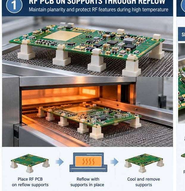
Radar PCB assembly release begins by treating heat, solder, cleaning, and mechanical force as RF variables. An RF board can leave fabrication within drawing limits and still change during paste printing, reflow, shielding, cleaning, or mechanical assembly. That risk is amplified in short-range and imaging radar front ends where antenna phase error, launch repeatability, and...

A Ground-Return Strategy for Radar PCB Antenna Transitions

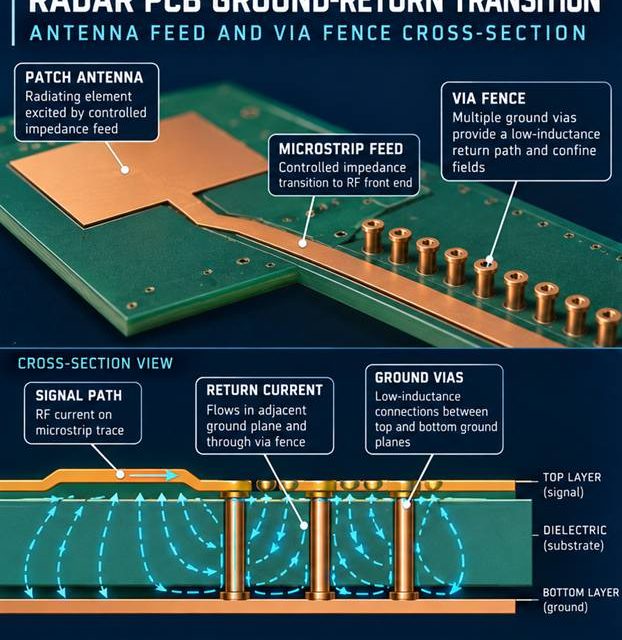
Radar PCB launch design begins with a complete three-dimensional signal and return path. The boundary between a board and a connector, coax, antenna, or shield is where a clean schematic becomes a three-dimensional electromagnetic problem. In short-range and imaging radar front ends where antenna phase error, launch repeatability, and thermal drift all affect detection margin,...

How a Radar PCB Stackup Preserves Phase Consistency Across the Array

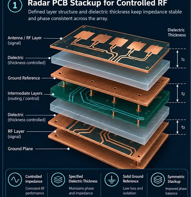
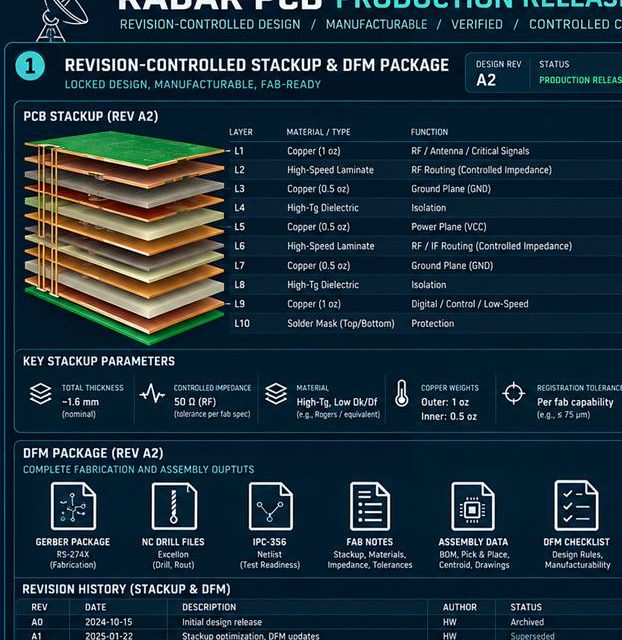
Radar PCB stackup release begins by making every electromagnetic and manufacturing assumption visible. Stackup discussions fail when the drawing lists layer names but not the electromagnetic and manufacturing assumptions behind them. In short-range and imaging radar front ends where antenna phase error, launch repeatability, and thermal drift all affect detection margin, the board must carry...

Radar PCB Design: Materials, High-Frequency Layout Techniques & Applications

Radar PCB: Design Principles, Materials, Manufacturing Challenges & Key Applications High-speed PCBs stand at the top of modern circuit-board technology, spanning digital high-speed, mixed-signal, and RF/microwave categories. Among these, RF and microwave PCBs operate at the highest frequencies, making them essential for advanced applications—especially RADAR (Radio Detection and Ranging). Because Radar PCBs frequently host a...