
Radar PCB fault isolation begins at the physical boundary where the symptom is reproduced. A short-range and imaging radar front ends where antenna phase error, launch repeatability, and thermal drift all affect detection margin can pass a schematic review and still fail in the chamber, the enclosure, or the vehicle. The failure often appears as a receiver sensitivity loss, an unstable calibration value, or a link that works only after the board is pressed into its housing.
For Radar PCB, the useful question is not whether one trace is “correct”; it is which physical reference, transition, or thermal movement changed between design intent and the assembled product.
This field-debugging guide gives an engineering team a repeatable way to separate layout, material, fabrication, and integration causes without inventing a measurement result.
Use the Radar PCB release as a controlled engineering object: the board, stackup, fabrication note, assembly recipe, and verification record must describe the same physical path. The guidance below is intentionally practical; it separates a design target from a supplier typical value and keeps any inference visible.
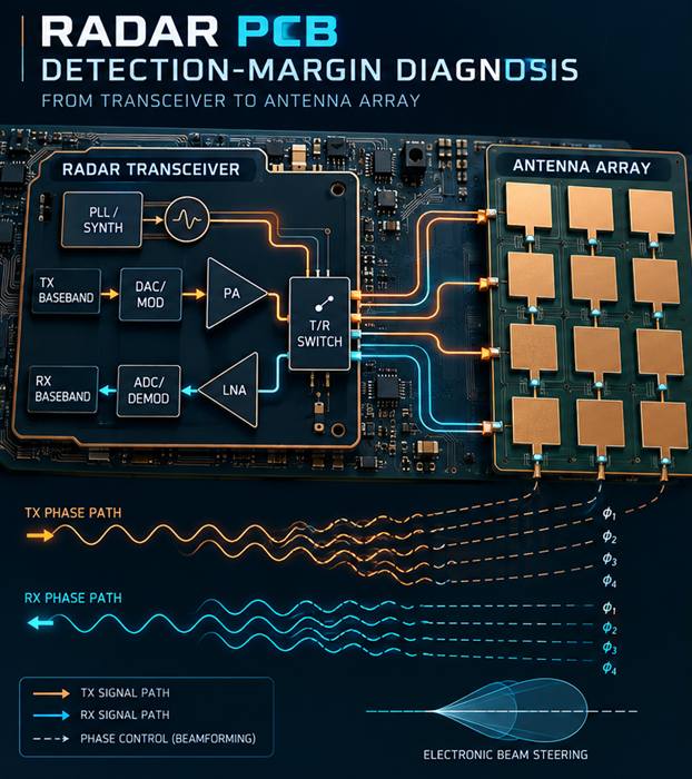
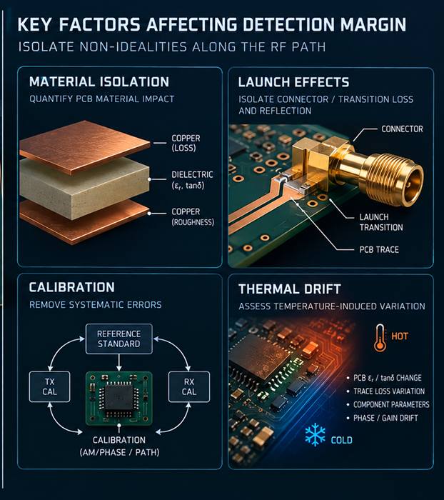
Table of Contents
Radar PCB — Start with the symptom map
Record the failure in the same units and operating state that the product team used to reproduce it. A module that loses 1 dB of link margin at one temperature is a different problem from a board that fails only after a connector is mated twice. Mark the radio channel, enclosure state, supply mode, antenna port, firmware build, and assembly lot. This converts a vague “RF issue” into a boundary condition. A short symptom map should distinguish a constant offset, a frequency slope, a temperature slope, and a unit-to-unit spread. Each pattern points toward a different suspect: copper roughness and dielectric loss often create frequency slope; reference-plane discontinuity creates a localized notch; connector seating produces intermittent spread; and warpage or moisture creates temperature history. The project file should cross-reference multilayer PCB and PCB materials so the same constraint is visible to both design and sourcing. The controlled release record for this section is Radar PCB; use the linked page as the internal capability reference while the article supplies the engineering decision.Separate the launch from the line
The fastest isolation step is to treat the connector or antenna launch as a complete system rather than inspecting only the signal width. Check pad geometry, antipad, nearby ground vias, the return-current path on the first reference plane, and the distance from the transition to the enclosure or shield. For Radar PCB, the launch should be reviewed against the finished stackup, not the nominal CAD material name. A via that looks centered in a 2-D view can force current around a void in the reference plane, adding inductance that becomes visible only at the upper band edge. Use a coupon or fixture that reproduces the same launch geometry; a generic coupon may prove the laminate is acceptable while missing the actual product discontinuity. A practical handoff also names RF PCB design, controlled impedance PCB, and PCB manufacturing where those terms describe the physical feature being released. The controlled release record for this section is Radar PCB; use the linked page as the internal capability reference while the article supplies the engineering decision.
Use the material and plane as evidence
If the launch is repeatable, inspect the build records for dielectric thickness, copper foil type, resin content, pressed thickness, and the controlled impedance target. Do not replace a supplier value with a guessed single Dk number. For Radar PCB, the useful control is often a range tied to frequency and glass style, plus a measured or released laminate construction. Compare the drawing to the build traveller and to the panel cross-section. If the board uses mixed dielectric families, look for a transition where the RF line changes field distribution. Moisture conditioning and solder-mask registration can also alter the effective geometry. A production review should therefore combine PCB materials with controlled impedance PCB rather than treating them as separate documents. Keep PCB assembly beside the drawing revision, and use high-reliability PCB for the verification owner rather than leaving the requirement in email. The controlled release record for this section is Radar PCB; use the linked page as the internal capability reference while the article supplies the engineering decision.Close the loop with a controlled re-test
After one physical variable is changed, repeat the same fixture, torque, temperature soak, and calibration sequence. Changing the cable, software, and board revision together produces an attractive graph but no diagnosis. Use a small matrix: nominal unit, suspect unit, alternate connector, and one board with the return path repaired. The goal is a directional decision, not a fictional customer “case study.” Record whether the defect follows the board, the fixture, the connector, or the environment. When the issue follows the board, ask manufacturing to inspect drill registration, plating continuity, solder-mask pullback, and copper balance. The PCB manufacturing release should carry these observations as acceptance evidence. The manufacturing traveller can then connect signal integrity with DFM review and preserve evidence for the next lot. The controlled release record for this section is Radar PCB; use the linked page as the internal capability reference while the article supplies the engineering decision.
Decision for the project manager
Do not approve a layout respin because a single sweep looks better. Approve it when the team can state which variable moved, why that variable is inside the supplier process window, and how the next lot will be screened. For Radar PCB, the handoff should identify the RF path, reference plane, launch geometry, material construction, and the re-test condition. If the data cannot distinguish design from assembly, keep the item at engineering hold and schedule a focused coupon or fixture check. That decision protects schedule better than allowing several uncontrolled “small improvements” to enter the next build. Before sign-off, confirm RF front-end PCB and thermal management PCB are linked to the same revision and acceptance method.Release checklist for the next build
- State the operating band, enclosure state, and environmental boundary for Radar PCB.
- Identify the controlled material construction, copper profile, and pressed dielectric tolerance.
- Show the complete signal and return path through connectors, vias, shields, and planes.
- Tie fabrication and assembly checks to a revisioned drawing, coupon, or inspection record.
- Label typical values, design targets, engineering ranges, and measured values separately.
- Record the owner and closure evidence for every open RF, thermal, and mechanical risk.
