HomeCategory

PCB Manufacturing Services | High-Quality PCB & PCBA - KKPCB

PTFE PCB DFM: Panelization and Procurement Controls for Repeatable RF Builds

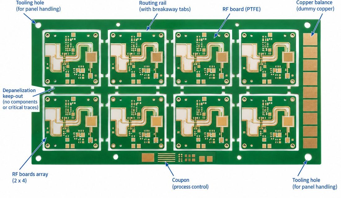
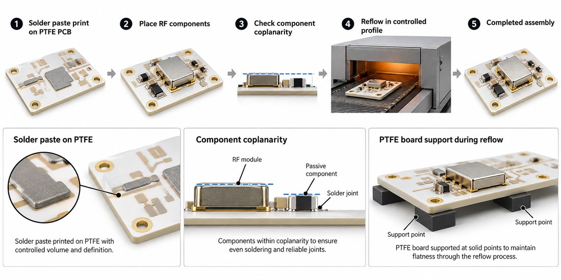
A PTFE board can be electrically well designed and still be difficult to quote or panelize. The manufacturing risk is concentrated at the interfaces: copper balance, drilled features, plated edges, hybrid stackup boundaries, connector rails, and the coupon that is supposed to represent the RF path. A PTFE PCB release should therefore explain the process...
PTFE PCB Loss Budgets: Copper Profile Checks for Long RF Paths

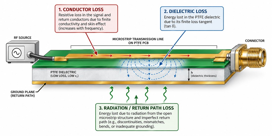
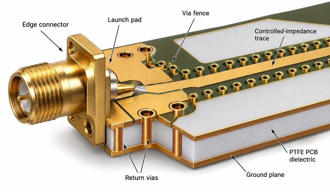
When a microwave path becomes long enough, the material name alone cannot explain insertion loss. A PTFE PCB combines dielectric loss, conductor roughness, trace geometry, resin or ceramic loading, connector transitions, and the return path. Engineers often discover the real problem during a system margin review because the original estimate used a catalog loss tangent...

Ceramic PCB CTE and Moisture Decisions for Outdoor Radar and Sensor Modules

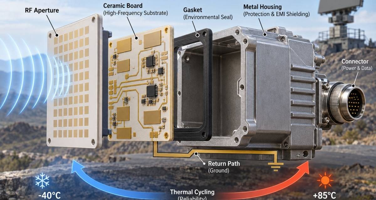
Outdoor radar and sensor hardware sees temperature swings, condensation risk, vibration, and repeated enclosure loads. A Ceramic PCB can reduce some dimensional and moisture-related uncertainty, but it does not remove the need to coordinate the ceramic, copper, seal, connector, and metal housing. The project pain appears when a material is chosen for a nominal dielectric...

Ceramic PCB Metallization and Via Reliability: A Practical Review for RF Power Boards

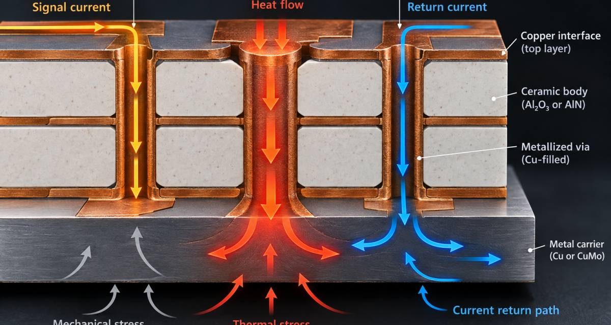
A ceramic substrate can be electrically stable and thermally efficient while the interconnect still becomes the weak point. Metallization adhesion, plated or filled vias, copper thickness, and the transition to a connector or carrier all experience different mechanical strain. For a Ceramic PCB used in a power or microwave module, the correct question is not...

Ceramic PCB Antenna Cavities at mmWave: Controlling Geometry Before the First Build

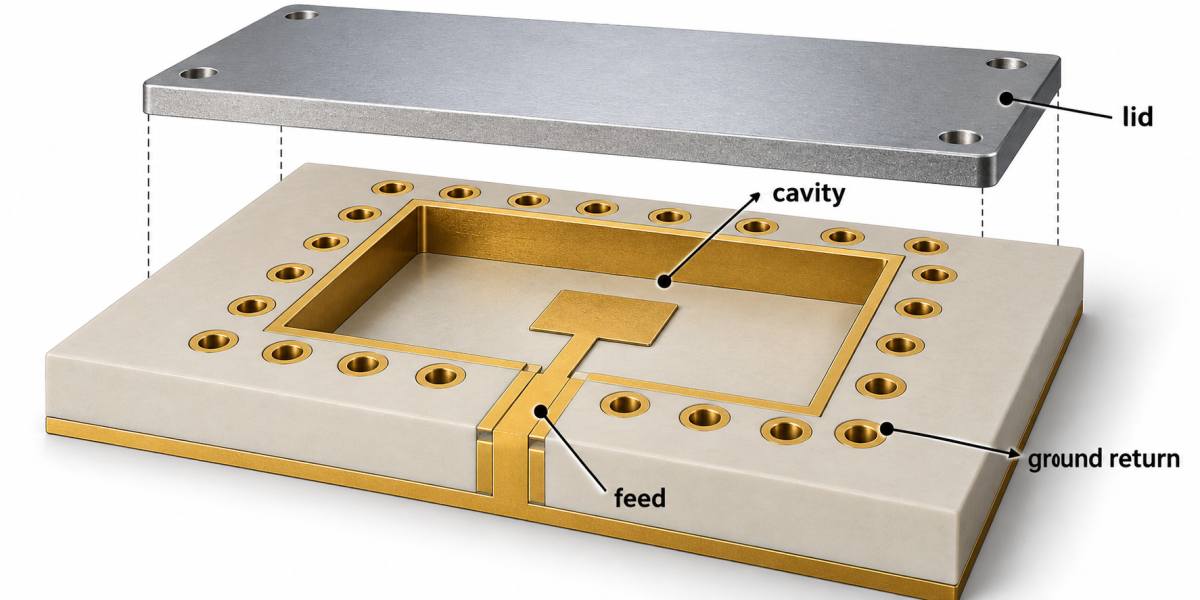
At mmWave frequencies, the cavity, copper edge, connector launch, and antenna clearance become part of the circuit. A Ceramic PCB is often selected for its dimensional stability and integration potential, yet a cavity that is only slightly too deep or a ground fence that is interrupted by a tooling keep-out can move the resonance enough...

Ceramic PCB Thermal Interfaces for High-Power RF Modules: A Release Review

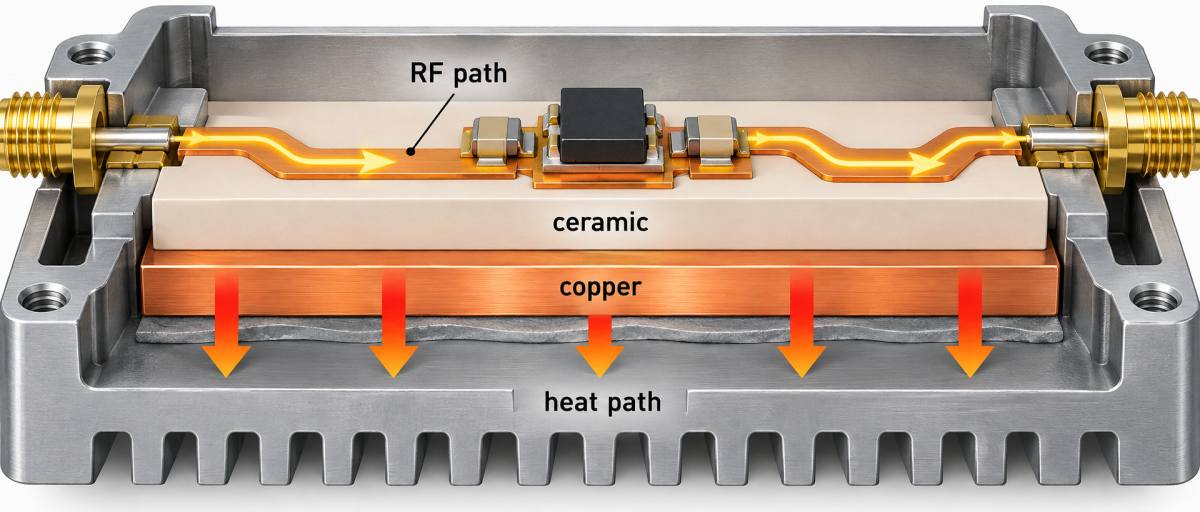
A high-power RF module can meet its electrical target and still fail in the field because the heat path was never released as a complete system. A Ceramic PCB changes the design conversation: the ceramic substrate, copper pattern, attach method, via or metallized interface, and the enclosure all share the same thermal boundary. The project...

Ceramic PCB DFM and Procurement Release: Avoiding First-Build Surprises

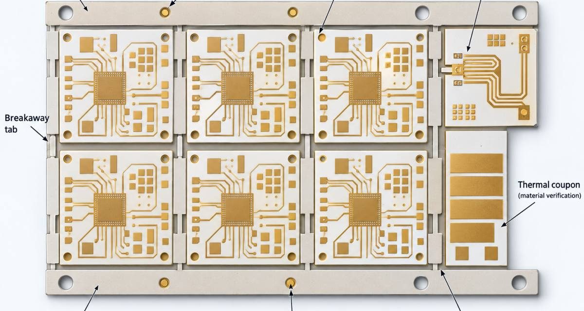
Ceramic PCB programs often move from concept to purchase order faster than the manufacturing package matures. The layout may be complete, but the supplier still lacks a defined panel, edge condition, metallization note, inspection plan, or approved substitute rule. That gap creates schedule risk because a ceramic panel is not interchangeable with a conventional laminate...

Megtron 7 PCB DFM Release: Panelization, Coupons, and ECO Control Before Volume Build

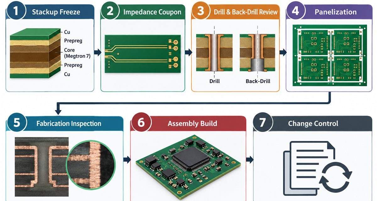
The most expensive Megtron 7 PCB problem is often a release problem, not a material problem. A prototype may route correctly, yet the volume panel has no representative coupon, uneven copper, an impractical depanelization rail, or an ECO that quietly changes the impedance construction. A useful DFM gate turns the electrical intent into a package...