HomeCategory

PCB Design Services | Professional PCB Layout & Design - KKPCB

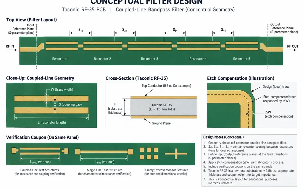
Taconic RF-35 PCB for RF Filters: Reliable Coupled-Line Geometry Through Fabrication

Taconic RF-35 PCB coupled-line filter performance is governed by geometry that fabrication can actually hold. The filter designer may calculate a narrow gap and exact line length, but etch bias, copper profile, dielectric thickness, plating, and solder mask decide whether the finished board has the intended coupling. That is why a filter release needs more...
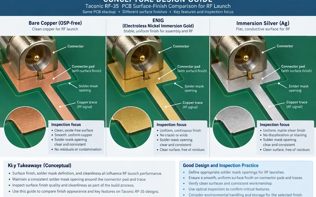
Taconic RF-35 PCB Surface Finish Choices for Consistent RF Launches

Taconic RF-35 PCB surface finish selection is a launch-interface decision, not a procurement checkbox. A finish changes pad topography, solder wetting, contact behavior, and the geometry the RF current sees at the connector or package transition. The project pain appears when a finish is changed after layout release and the team has no coupon or...

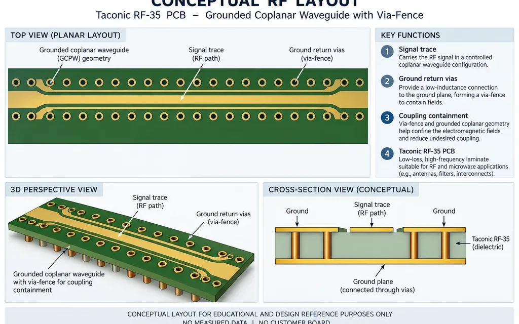
Taconic RF-35 PCB Ground Via Fences: Reliable Coupling Control in Dense Wireless Modules

Taconic RF-35 PCB via fence coupling control is a layout-and-fabrication problem. A fence can contain a field only when its pitch, plane connection, anti-pad, and registration match the frequency range and stackup. In a dense wireless module, an apparently complete row can still leak through a split plane, connector keep-out, or drill offset. Table of...

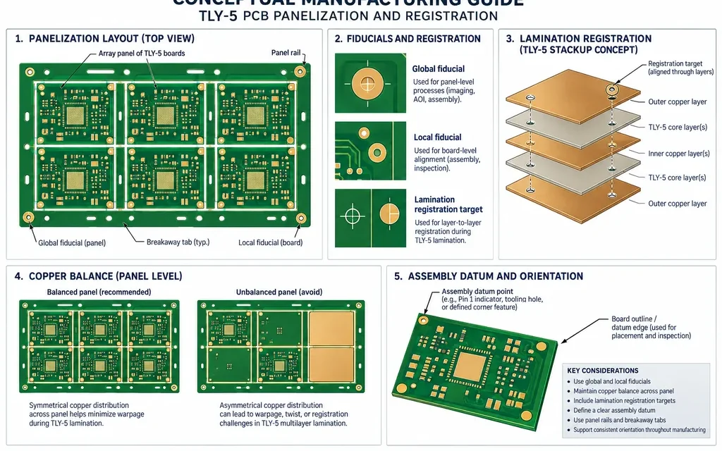
TLY-5 PCB Panelization: A Robust Registration Strategy for RF Assembly

TLY-5 PCB panelization registration is a project risk when a low-Dk RF design is copied into a manufacturing panel without considering press flow, copper distribution, routing, and assembly tooling. The board may be electrically correct as an individual drawing yet lose connector alignment or channel-to-channel phase consistency after it is nested, laminated, routed, and depanelized....

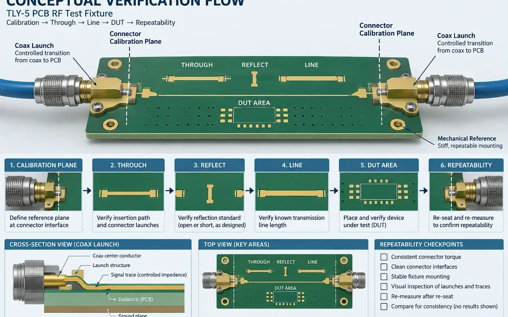
TLY-5 PCB RF Test Fixtures: A Reliable Calibration and Connector Interface Workflow

TLY-5 PCB RF test fixture design is often the hidden variable in a prototype program. A device under test can appear to have excess loss or phase drift when the real variation comes from connector wear, launch geometry, cable movement, or an undefined calibration plane. The fixture must be treated as an RF product with...

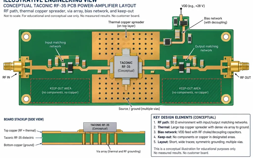
Taconic RF-35 PCB Power Amplifier Layout: A Robust Heat-Spreading Path That Protects RF Tuning

Taconic RF-35 PCB power amplifier thermal work must preserve two things at once: the device must shed heat, and the RF path must keep its intended impedance and return current. The common project failure is a late copper pour or thermal-via change that improves a temperature estimate but shifts the launch, bias isolation, or local...

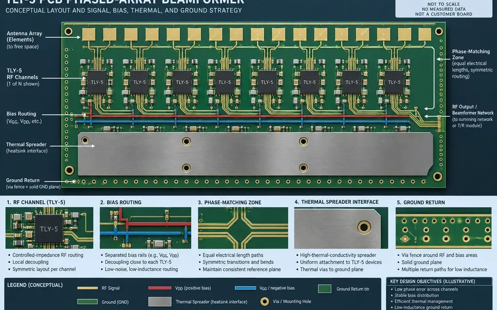
TLY-5 PCB in Phased-Array Beamformers: A Thermal and Bias-Routing Strategy

TLY-5 PCB beamformer thermal design is a coupled RF and power problem. In a phased array, each channel must preserve phase while bias networks, power amplifiers, control lines, and heat paths share a compact multilayer board. The engineering risk is not simply a hot spot; it is a hot spot that changes dielectric geometry, connector...

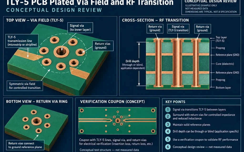
TLY-5 PCB Via Fields: Designing Plated Transitions Without Tuning Away the Real Problem

A TLY-5 PCB via field is not a cosmetic layout detail in a Ku-band module. The plated transition decides where the return current closes, how much barrel remains beyond the active layer, and whether the connector launch modeled by the RF team still represents the finished board. When this is released late, the first prototype...

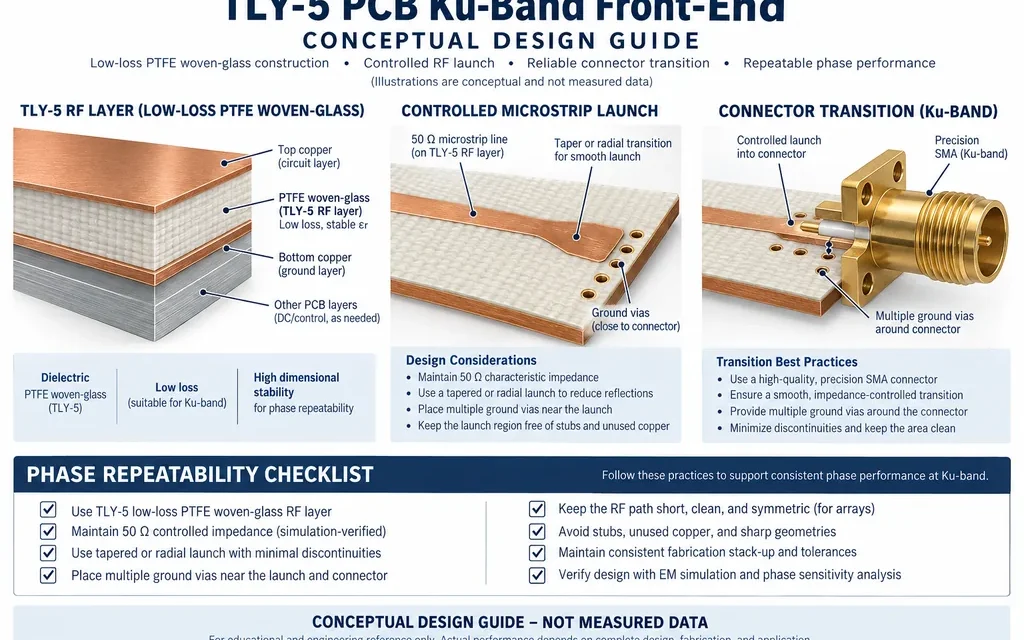
TLY-5 PCB for Ku-Band Front Ends: Managing Copper Roughness and Phase Repeatability

Ku-band TLY-5 PCB projects need a finished-board reference, not only a laminate name. Table of Contents Finished-board sensitivity Copper roughness Connector launch Phase repeatability Manufacturing handoff Release checklist TLY-5 PCB is often selected for a Ku-band front end because the laminate combines a low nominal dielectric constant with low dielectric loss. The difficult part is...

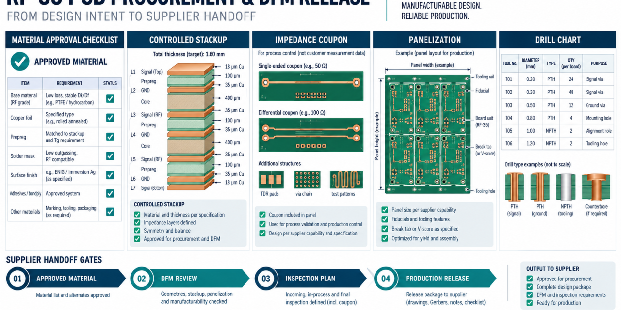
RF-35 PCB Procurement and DFM: A Supplier-Ready Release Checklist

Procurement teams often receive a microwave PCB package that looks complete but leaves the fabricator to guess the laminate grade, pressed dielectric, coupon method, or drill sequence. This supplier-ready checklist uses an RF-35 PCB example to turn design intent into controlled purchasing and DFM inputs without inventing customer results. RF-35 ceramic-filled PTFE/glass laminates are commonly...