
Taconic RF-35 PCB via fence coupling control is a layout-and-fabrication problem. A fence can contain a field only when its pitch, plane connection, anti-pad, and registration match the frequency range and stackup. In a dense wireless module, an apparently complete row can still leak through a split plane, connector keep-out, or drill offset.
Table of Contents
Define what the fence is supposed to contain
Separate aggressor and victim paths, connector launches, antenna feeds, or a noisy digital island before choosing pitch. Taconic RF-35 PCB stackup and frequency assumptions should state whether the fence is a wall, a return-current bridge, or a local shield. The RF PCB design design review can then assign a measurable spacing and plane-connection rule instead of a generic “stitch every grid.”
Connect the fence to the correct reference plane
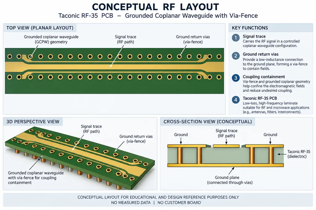
A via connected to the wrong layer can look present while leaving the intended return path open. Check signal layer, reference plane, anti-pad, and nearby copper in cross-section. Taconic RF-35 PCB ground vias should be dimensioned from the same datum as the launch. The PCB manufacturing manufacturing traveler should carry drill table, finished hole, annular-ring, and registration requirements together.
Respect connector and assembly keep-outs
Fences often stop near connectors, shields, stiffeners, or fasteners. That gap can become the dominant coupling path. Taconic RF-35 PCB RF PCB materials and finished thickness should be modeled at the gap, not only in the uniform section. The RF PCB materials assembly drawing should identify shield solder, connector body, cleaning access, and rework limits that could force a fence interruption.
Use a witness that represents the gap
A long uniform via row is a weak coupon. Put a split, connector-like gap, and reference-via arrangement into the witness structure. Taconic RF-35 PCB coupon data should use the same layer pair and finish. The controlled-impedance PCB controlled-impedance PCB review can compare coupling, return loss, and cross-section evidence with the geometry that actually failed or passed.
Release the fence with inspection points
Freeze pitch, drill, anti-pad, plane connection, gap rule, and cross-section location. Label calculations and targets separately from any measured coupling result. Taconic RF-35 PCB documentation keeps the fence tied to the product intent. The PCB assembly manufacturing record should identify panel position, drill revision, copper balance, and any local repair before RF evaluation.
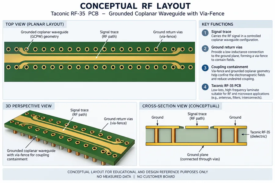
The useful output is not “more vias.” It is a fence whose electrical role, mechanical datum, drill class, and inspection evidence are all visible. That is the level of definition needed to move a wireless module from a promising simulation to a stable production release.
Project evidence and handoff for Taconic RF-35 PCB via fence coupling
For a via-fence design, retain the aggressor-victim map, plane connection, pitch, anti-pad, gap rule, drill class, cross-section, and coupling acceptance window. The record should explain why each fence segment exists and what happens at connector or shield interruptions. The Taconic RF-35 PCB drawing should make the critical datum visible to layout, fabrication, assembly, and test. If a number is calculated, retain the assumptions; if it is a supplier typical, keep it labeled as typical; if it is a measured acceptance value, keep the sample, method, and revision traceable.
| Release item | Engineering question | Evidence to retain |
|---|---|---|
| Stackup and material | Does the finished construction match the RF model? | Finished dielectric target, copper assumption, material lot, cross-section |
| Transition or critical path | Is the mechanical datum also the electrical datum? | Launch drawing, via or pad dimensions, mask and connector inspection |
| Process witness | Does the coupon represent the product feature? | Panel position, layer pair, finish, drill and impedance record |
| Assembly and test | Could placement, rework, or calibration move the result? | Placement tolerance, reflow or rework history, fixture and reference plane |
For program control, use a short disposition statement after each build: what passed, what moved, what is still a target, and which owner decides the next change. This keeps the Taconic RF-35 PCB via fence coupling discussion focused on evidence and prevents a new material, finish, or layout change from being introduced without an updated model and acceptance plan.
Sources: Taconic and Rogers typical material data; IPC-TM-650 methods relevant to dielectric, copper, drilling, plating, registration, and impedance; RF application guidance from Qorvo, Analog Devices, and Würth Elektronik; KKPCB PCB design, materials, manufacturing, assembly, and high-frequency capability pages. Values are typical, target, or calculated references unless explicitly identified as measured.
