
Procurement teams often receive a microwave PCB package that looks complete but leaves the fabricator to guess the laminate grade, pressed dielectric, coupon method, or drill sequence. This supplier-ready checklist uses an RF-35 PCB example to turn design intent into controlled purchasing and DFM inputs without inventing customer results.
RF-35 ceramic-filled PTFE/glass laminates are commonly specified for RF and microwave circuits. Current supplier tables give typical values such as Dk near 3.50 at 1.9 GHz and a low dissipation factor; procurement should treat them as reference values and require the approved datasheet, lot traceability, and finished-stackup agreement before release.
1. Lock the RF-35 PCB technical inputs
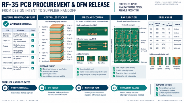
Start with a single controlled material list. Name the RF-35 grade, core or prepreg construction, copper foil type, finished thickness, surface finish, solder mask restrictions, and any approved alternate. If the purchase order says only “RF-35,” the supplier may not know whether the design assumes a particular glass style or pressed dielectric height.
- List the approved manufacturer and material revision.
- State the target impedance, tolerance, and critical RF layer pair.
- Identify connector launches, via fences, back-drill features, and controlled-depth holes.
- Separate typical material properties from project acceptance values.
A high-frequency PCB request should also include the operating band, connector family, loss budget, and assembly profile. These details let the fabricator check whether the proposed stackup is electrically sensible and manufacturable before quoting.
2. Approve the stackup and impedance coupon
For an RF-35 PCB, the stackup is a purchasing document as well as an electrical model. It should show layer order, finished copper, pressed dielectric targets, reference planes, impedance classes, and the coupon location. A coupon built from a different core, copper state, or press construction cannot fully represent the product.
| Release document | Minimum content | Owner at handoff |
|---|---|---|
| Material list | Grade, thickness, supplier, alternate, lot record. | Procurement and engineering. |
| Stackup drawing | Layer order, copper, dielectric, impedance pair. | Design and fabrication. |
| Drill chart | Finished sizes, plated types, back-drill notes. | Fabrication engineering. |
| Coupon plan | Representative geometry and acceptance method. | Quality and test. |
Use the approved PCB design files to verify that the line geometry matches the pressed dimensions. If a supplier proposes a different RF-35 PCB core or prepreg combination, update the model and drawing together instead of approving a verbal substitution.
3. Run the DFM gate before tooling
DFM review should connect geometry to the supplier’s actual process. Check annular ring, minimum drill, aspect ratio, copper balance, layer registration, solder-mask clearance, edge routing, panel rails, fiducials, and depanelization. RF launches need an additional check for via-fence pitch, antipad clearance, connector seating, and reference-plane continuity.
For an RF-35 PCB, ask the fabricator to identify which dimensions are nominal targets and which are guaranteed acceptance limits. This prevents a common procurement error: treating a catalog thickness or a simulator output as a finished-board tolerance. KKPCB can review the stackup, propose a buildable sequence, and flag constraints before tooling and material are committed.
4. Define inspection and acceptance
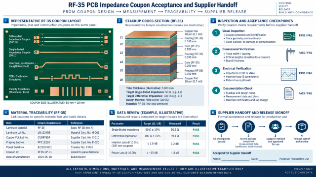
The inspection plan should state incoming material checks, cross-section review, dimensional registration, plated-hole quality, impedance method, and documentation retention. A TDR or VNA plot is meaningful only when the fixture, calibration, coupon ID, and test revision are recorded. Do not label an illustrative waveform as measured customer performance.
A PCB manufacturing traveler should link every inspection checkpoint to the same revision-controlled stackup. If the product needs environmental or thermal cycling, define the sample count, conditioning profile, and acceptance criteria before the build. Those criteria are project decisions, not generic RF-35 PCB marketing claims.
5. Complete the supplier handoff
The final package should contain Gerbers or ODB++ data, drill files, stackup, impedance table, fabrication notes, panel drawing, coupon drawing, inspection plan, approved material list, and assembly restrictions. Give the PCB assembly team the same connector, mask, paste, shield, and no-rework notes used by fabrication.
For demanding multilayer programs, KKPCB states capability up to 62 layers and 8 sequential lamination steps. That capability can support complex RF/digital builds, but procurement still needs a realistic panel outline, lead time, and inspection route. In summary, a reliable RF-35 PCB purchase is achieved when material, geometry, DFM, coupon, and acceptance language are aligned before the purchase order is released.
Sources: Taconic RF-35 and RF-35P processing guidance and typical property tables; IPC-TM-650 references for impedance, dimensional, and microsection evaluation; and KKPCB manufacturing capability notes. Typical values are reference data rather than customer measurements; confirm the current supplier datasheet and lot before release.
