
Engineering intent. A 77 GHz radar front end is sensitive to the geometry between the antenna elements, feed transitions, and transceiver. This article explains how to plan a RO3003 PCB stackup for that path. It is a conceptual design workflow, not a customer case study or a measured production result.
RO3003 is a ceramic-filled PTFE laminate in the Rogers RO3000 family. Rogers lists a nominal design dielectric constant of about 3.00 for RO3003 under specified test conditions and describes stable dielectric behavior over temperature and frequency. The value used in an impedance or phase model must still match the supplier test method, copper profile, and finished dielectric thickness.
Why a 77 GHz feed changes the stackup decision
At automotive radar frequencies, a small change in electrical length can shift phase balance between antenna channels. A route that looks short in the CAD view may include a connector launch, via field, pad breakout, and bend that all contribute to phase and loss. The stackup therefore becomes an RF architecture decision instead of a late fabrication detail.
Start by defining the antenna topology, channel count, launch type, and whether the transceiver sits on the same layer as the array. If a design uses a patch array, the antenna layer must be separated from noisy digital routing. If it uses a connector to a remote antenna, the connector geometry and reference transition must be included in the model.
Translate the radar requirement into stackup inputs
A fabrication-ready RO3003 PCB stackup should state the controlled layer, nominal and finished dielectric thickness, copper weight, foil type, and reference plane. These items determine the impedance and phase velocity more directly than a material name alone.
| Stackup input | Engineering question | Release note |
|---|---|---|
| Dielectric thickness | What finished spacing gives the required line width and coupling? | Show nominal and tolerance after lamination. |
| Copper foil and profile | How will etch profile and roughness alter the high-frequency model? | Record foil family and any roughness assumption. |
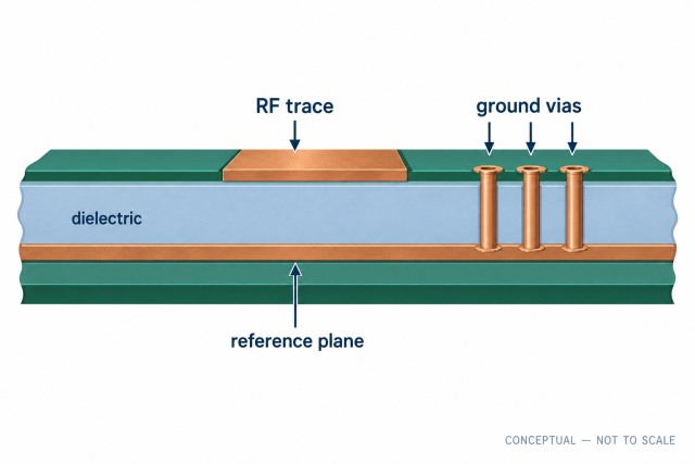
| Reference plane | Does every feed segment have a continuous return path? | Mark voids, slots, and keepouts on the layout drawing. |
| Via transition | Will the transition create a stub or an abrupt field change? | Define back-drill, antipad, and nearby ground vias if needed. |
Use the same construction in the field solver, PCB layout library, fabrication drawing, and purchasing specification. If the fabricator proposes a different press construction, recalculate the controlled impedance and phase length before approving the change.
Choose the transmission-line form before routing
Microstrip for exposed antenna structures
Microstrip can be appropriate for an antenna layer when the conductor-to-plane spacing is tightly controlled and the enclosure allows the field distribution. Its width is influenced by dielectric thickness, copper thickness, solder mask, and the actual effective dielectric constant. Do not copy a trace width from a generic online calculator without checking the released stackup.
Grounded coplanar waveguide for transitions
Grounded coplanar waveguide can help manage launches and provide a defined lateral return path. The trace-to-ground gap, via-fence pitch, pad shape, and component clearances are all part of the structure. A controlled impedance PCB review should therefore include the complete cross-section and the top-view fence geometry.
Handle antenna feeds, vias, and phase balance
Keep each array branch referenced to the same plane and avoid unnecessary layer changes. When a layer change is unavoidable, use a compact signal via with nearby ground vias and remove unused via barrels where the design requires it. The exact dimensions are design outputs, not universal rules; they depend on the stackup and the package or connector footprint.
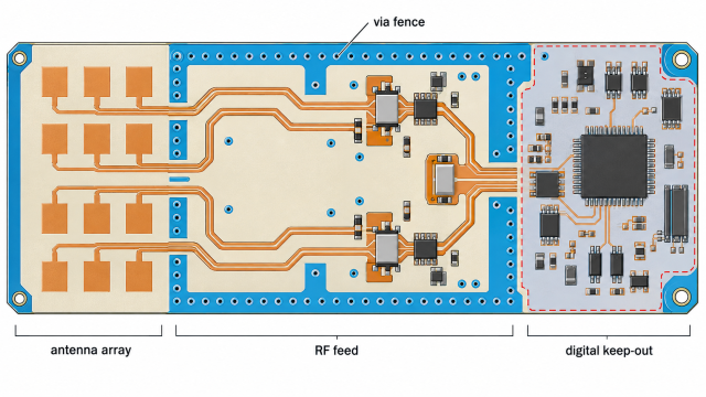
For equal-phase channels, route branches with the same transmission-line form and avoid mixing wide microstrip sections with narrow coplanar sections without a transition model. Match electrical length rather than only centerline length. A conceptual phased-array example should be labeled as a target design, not as a measured result from KKPCB production.
Place the antenna elements, feed splitters, and transceiver boundary before routing digital clocks. Keep switching regulators, memory buses, and high-current return paths outside the antenna current region. The RF PCB capability review should check whether the proposed layer order can be manufactured with the required registration and via tolerances.
Plan manufacturability around the material
RO3000 fabrication guidance supports standard double-sided and multilayer PTFE processing, but the board house still needs clear instructions for surface preparation, drilling, lamination, and copper treatment. A high-frequency PCB materials review should confirm availability, thickness options, copper choices, and compatibility with the rest of the build.
Before release, ask the fabricator to review:
- the finished dielectric targets used in the impedance model;
- the drill and back-drill capability for the selected via structures;
- the registration budget between antenna, signal, and plane layers;
- the copper surface and etch assumptions used in loss estimates; and
- the coupon or inspection method that will verify the controlled feature.
These checks do not create a measured radar result. They make the design intent visible so that a prototype can be evaluated against a defined target.
Verification plan for the first radar prototype
Verification should connect the stackup to the real antenna, radome, connector, and enclosure. Review the feed return loss, channel-to-channel phase balance, and any coupling into the digital section using the agreed fixtures and acceptance limits. If the design uses a supplier typical Dk value, record it as a model input, not as a guarantee of finished-board performance.
| Review gate | Evidence to collect | Decision |
|---|---|---|
| Pre-layout | Material construction, line form, and target impedance | Approve the stackup model. |
| Layout | Return paths, via fences, phase-length rules, and keepouts | Approve the RF geometry. |
| Fabrication | Press construction, drilling notes, and coupon plan | Release to build. |
| Prototype | Fixture-based RF checks and system-level radar validation | Compare with requirements. |
KKPCB can review the PCB manufacturing services requirements against the released stackup and flag changes before fabrication. The useful outcome is a traceable build definition, not a claim that every RO3003 PCB will behave identically in every radar enclosure.
Sources: Rogers RO3000 Series Laminates product information; Rogers RO3000 laminate data sheet for RO3003; Rogers fabrication guidelines for RO3000 and RO3200 series high-frequency circuit materials. Supplier values are cited under their stated conditions and are not finished-board measurements.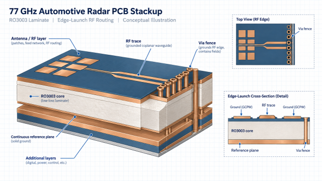
For a design review, document the exact RO3003 PCB construction, reference planes, and launch assumptions so the RF team and fabricator share the same baseline.
Before releasing a prototype, verify that the RO3003 PCB geometry remains consistent with the approved field model and the final drawing. A controlled revision history helps distinguish a conceptual target from a finished-board measurement.
When the stackup changes, reassess the RO3003 PCB build notes with the selected PCB layout rules and material availability.
The associated PCB layout review should record any phase-length, via-fence, and keepout changes before the next fabrication release.
