
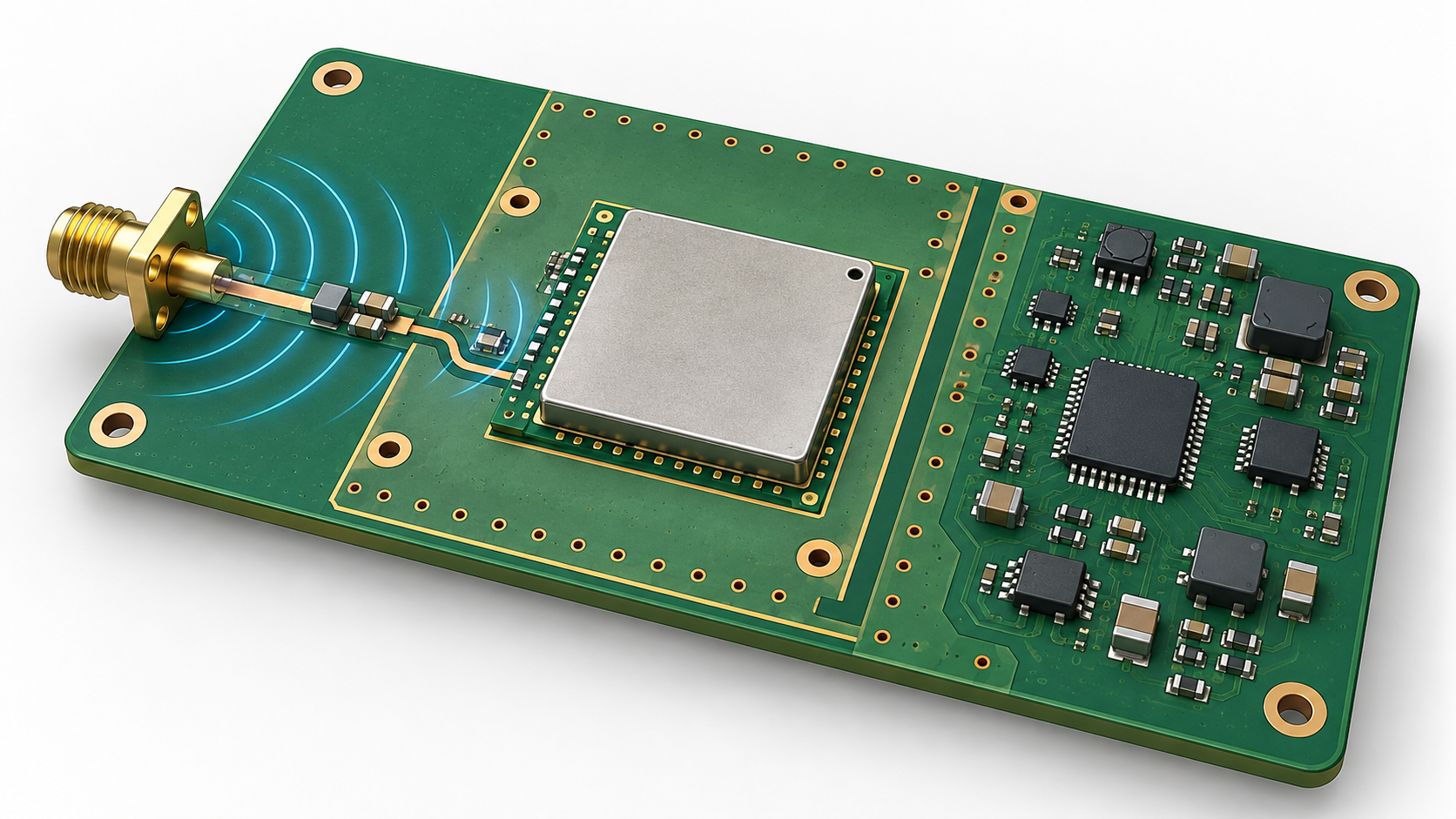
A GNSS module PCB is often treated as a simple carrier for a receiver module, antenna connector, and power supply. That view misses the part of the board that most often determines whether the receiver sees a usable signal: the path from the antenna to the module input. The layout must preserve the intended transmission-line impedance, provide a continuous return path, and keep switching noise away from the RF front end. It must also be documented well enough that the fabricated board matches the design model.
This article focuses on the pre-fabrication decisions for a GPS or multi-band GNSS receiver board. It does not replace the module vendor’s reference layout, antenna data, or regulatory requirements. Those documents remain the first design authority.
Define the receiver boundary before layout begins
Start by listing the exact receiver bands, antenna type, module input topology, and installation environment. GPS technical documentation identifies civil signals at L1, L2, and L5; their familiar center frequencies are 1575.42 MHz, 1227.60 MHz, and 1176.45 MHz respectively. A board for a single L1 active antenna has a different loss budget and filtering problem from a multi-band receiver, even if both are called GNSS modules.
Before the first trace is routed, capture the following information from the module and antenna documentation:
- the antenna feed impedance and whether the antenna is active or passive;
- the allowed matching network footprint and the recommended component placement order;
- the ground, keepout, and metal-clearance rules around the antenna and receiver;
- the receiver supply rails, oscillator requirements, and any RF shielding guidance; and
- the final enclosure, cable, and nearby noise sources.
These inputs prevent a common mistake: calculating a 50-ohm feedline for a generic stackup while the actual antenna, ground geometry, connector launch, or enclosure changes the RF environment.
Separate the RF path from noisy circuits
Place the antenna connector or antenna feed, input protection where required, matching footprint, and GNSS module so the RF path is short and direct. A continuous reference plane underneath the feed is usually more valuable than a cosmetically short route that crosses a split, a void, or a dense return-current path. Avoid routing the feed beside switch-mode inductors, fast digital clocks, display interfaces, or motor-control wiring. If the board also carries an RF PCB section, keep its return paths and shielding decisions explicit rather than relying on component placement alone.
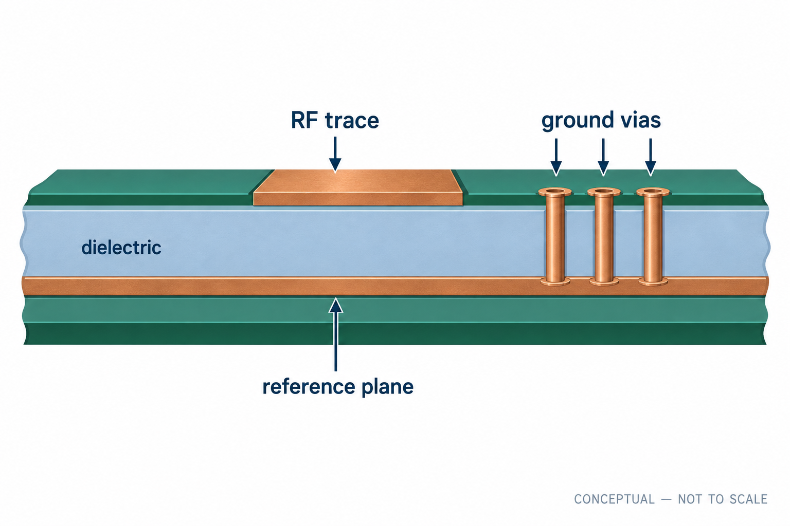
Ground-via stitching can help confine fields around a coplanar or microstrip structure, but it is not a substitute for a clean return plane. Keep any fence geometry, via clearances, and component pads inside the impedance model. The same applies to a connector launch: the transition into the board is part of the RF path, not an afterthought.
Choose the material and stackup from the actual RF problem
A GNSS module PCB does not automatically require an exotic microwave laminate. For a short, well-referenced feed at GNSS frequencies, a suitable FR-4 construction may meet the loss and impedance budget. Longer feedlines, tighter phase or temperature stability requirements, dense radio coexistence, and more demanding environments can justify a controlled high-frequency construction. The decision should come from the antenna-to-receiver budget and the fabrication model, not from a material name alone.
When a high-frequency laminate is selected, use the value that matches the supplier’s stated test method, frequency, material construction, and thickness. For example, Rogers lists typical 10 GHz process Dk values of 3.38 +/- 0.05 for RO4003C and 3.48 +/- 0.05 for RO4350B, with typical dissipation factors of 0.0027 and 0.0037 respectively. Those are material reference values, not finished-board measurements and not universal design inputs.
| Decision item | What the design team should specify | Why it matters |
|---|---|---|
| RF layer construction | Named laminate, nominal and finished dielectric thickness, copper weight, and foil type | These variables define the feedline impedance and loss model. |
| Reference plane | Continuous plane below the RF feed, with no unintended slots or crossings | Return-path discontinuities can change impedance and increase coupling. |
| RF transition | Connector launch, matching pads, vias, and their ground treatment | Each transition can introduce a discontinuity that a trace-width calculation does not capture. |
| Noise partitioning | Physical separation between the RF input and switching, clock, and high-current circuits | Receiver sensitivity can be limited by board-level coupling rather than feedline loss. |
Record the same construction in the simulation, fabrication drawing, and purchase specification. This keeps the RF model traceable when the material supplier, dielectric thickness, or copper finish changes.
Make the RF layout manufacturable
A controlled GNSS module PCB handoff should make the target impedance, return path, and material construction explicit before fabrication.
A 50-ohm callout is not enough for a fabricator to reproduce the feed. Provide the target impedance, the controlled layer, the trace geometry that may be adjusted, the required dielectric construction, and any critical tolerance. If the design uses a coplanar structure, define both the trace and ground gap. If the RF path changes layers, document the via transition and the intended ground-return treatment.
Use the final material stackup rather than a generic calculator result. Copper thickness, etch profile, dielectric thickness after pressing, and surface roughness can all move the effective transmission-line behavior. This is why high-frequency PCB work should include a stackup review before release, especially when the RF feed shares a board with dense digital or power circuitry.
A focused fabrication handoff
| Deliverable | Minimum content | Review question |
|---|---|---|
| Stackup drawing | Material family, layer order, copper thickness, dielectric thickness, and reference planes | Does it match the model used for the RF feed? |
| Impedance note | Target impedance, applicable layer, trace or gap dimensions, and allowed adjustment method | Can the fabricator identify the controlled structure without interpretation? |
| RF layout note | Antenna keepout, module reference-layout constraints, and no-copper or no-route areas | Are mechanical and enclosure constraints visible to layout and fabrication teams? |
| Verification plan | Prototype acceptance criteria and any required coupon, return-loss, or receiver-sensitivity check | Is the planned check tied to a design requirement rather than a generic test? |
KKPCB’s PCB materials page and PCB manufacturing services page provide the relevant material and fabrication context. Confirm the final material availability and the production capability against the released stackup rather than assuming a generic construction.
Verify the board in the same context in which it will operate
Prototype verification should reflect the real antenna, enclosure, cable, power mode, and nearby radios. Check the RF path before assuming a poor satellite lock is a firmware or module problem. A review that includes the antenna feed, the module reference layout, the ground path, the power-noise environment, and the released stackup is more useful than checking the PCB in isolation.
For a GNSS module PCB, the engineering objective is not to apply the most expensive material or the most complex stackup. It is to make the antenna-to-receiver path predictable, quiet, and reproducible from the first prototype through production. A final PCB layout review should keep the antenna feed, stackup note, and keepout constraints visible. The final GNSS module PCB release should make each controlled feature visible to layout, fabrication, and inspection.
Sources: GPS.gov technical documentation for GPS civil-signal documentation; Rogers RO4000 series laminate data for the cited typical material values and test conditions.
