
ADAS Sensor PCB — A vehicle program can report an intermittent reset, a communication dropout, a radar sensitivity loss, or a calibration value that moves only after the enclosure is closed. That symptom is not yet a PCB diagnosis. On a ADAS Sensor PCB, the board shares its boundary with a harness, connector, shield, heat path, and vehicle software state. This workflow helps the engineering team turn a field symptom into a controlled physical question without pretending that an unmeasured graph is a customer result. The release must make a distinction between a design target, a supplier typical value, an engineering range, and a measured value.
The steps below are a new engineering narrative for this product family, not a customer measurement or a copied case study.
Keep the ADAS Sensor PCB record joined to the drawing, stackup, fabrication note, assembly recipe, and verification plan. The same physical path should be named in every document so a late sourcing or housing change cannot quietly alter the vehicle behavior.
ADAS Sensor PCB — Start with the vehicle symptom, not the schematic
Capture the symptom with the operating state that made it repeatable: supply mode, vehicle network load, connector mating condition, firmware build, temperature history, and whether the housing or radome is installed. A short constant offset points to a geometry or loss issue; a frequency-dependent slope suggests conductor, dielectric, or reference-plane behavior; a failure after a vibration or thermal event raises connector, via, or warpage questions. For ADAS Sensor PCB, the first record should identify the exact interface and the boundary condition instead of using “RF problem” or “EMI problem” as a diagnosis.
The program file should cross-reference thermal management PCB and via design so design and sourcing see the same boundary. The released ADAS Sensor PCB page is an internal capability reference; the engineering decision remains in this article and the project file.
Split harness, power, and board evidence
Remove variables in a deliberate order. Compare a known-good harness with the suspect harness, a powered-down board with the same mechanical loading, and a connector mate cycle with torque or insertion force recorded. Check supply impedance and return current before changing the layout. The PCB assembly record is useful here because solder voids, shield contact, and rework history can create a spread that looks like a design defect. Keep every swap traceable to the same automotive PCB manufacturing lot.
The handoff should name surface finish PCB, turnkey PCB assembly, and PCB materials where those terms describe a controlled physical feature. The released ADAS Sensor PCB page is an internal capability reference; the engineering decision remains in this article and the project file.
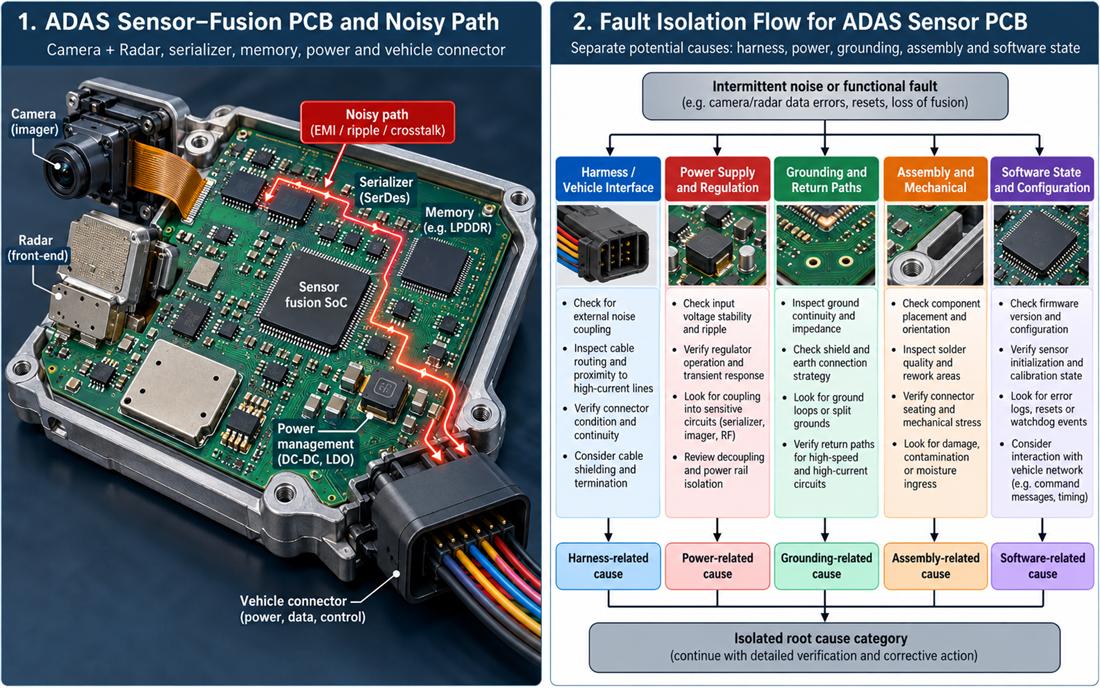
Read the stackup and return path
Once the symptom follows the board, inspect the physical RF and mixed-signal boundary: reference-plane gaps, connector antipads, via barrels, copper balance, solder-mask pullback, and the path from the power stage to the sensitive receiver or serializer. A material name alone does not prove the pressed dielectric thickness or copper profile. Record whether the value is a supplier typical, a design target, an engineering range, or a measured value. The PCB materials and controlled impedance PCB pages should support the released construction, not replace a cross-section review.
Keep high frequency PCB design beside the drawing revision and assign controlled impedance PCB as the verification owner. The released ADAS Sensor PCB page is an internal capability reference; the engineering decision remains in this article and the project file.
Replay the environmental trigger
Recreate the trigger one variable at a time. Use temperature soak, vibration fixture, connector force, supply transients, or enclosure compression only when they are part of the actual failure boundary. A 76–81 GHz radar board, for example, can respond to a small phase change that is invisible on a low-frequency continuity check, while a domain controller may fail because the return path or power plane changes under a shield frame. Repeat the same calibration and fixture setup; otherwise the team cannot tell whether the defect followed the board, harness, fixture, or environment.
The traveller can connect PCB manufacturing with PCB assembly and preserve evidence for the next lot. The released ADAS Sensor PCB page is an internal capability reference; the engineering decision remains in this article and the project file.
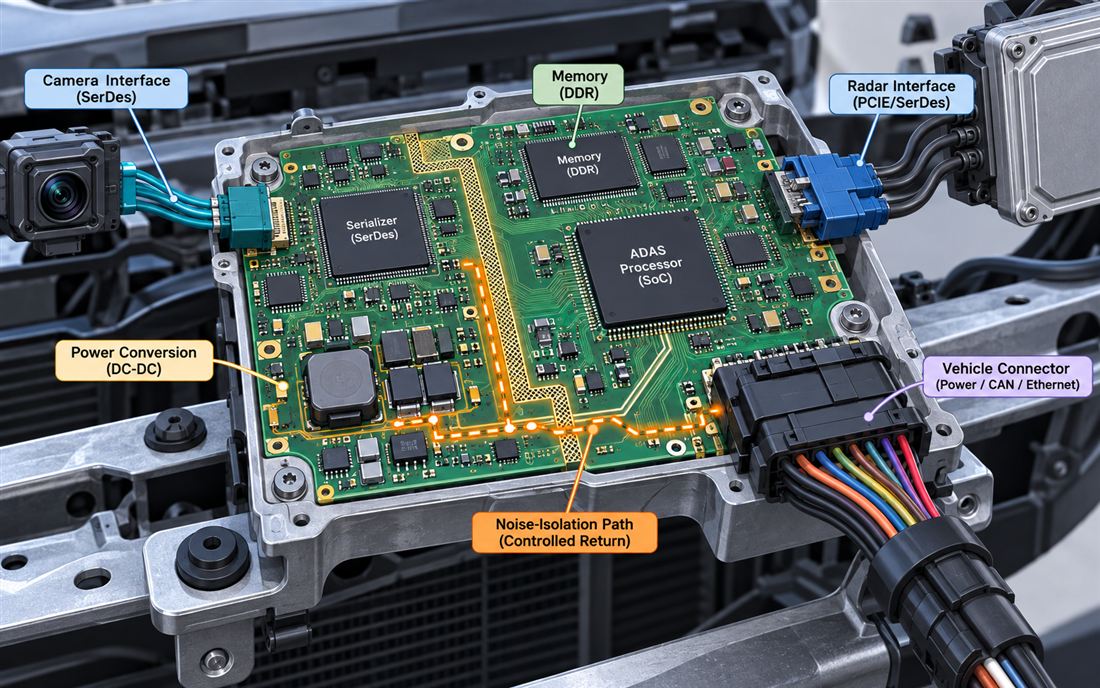
Choose containment before a redesign
Containment should state what is known and what is still open. Hold the affected lot if the defect follows a process step; issue a drawing correction if a controlled geometry is wrong; or keep an engineering hold if the evidence cannot distinguish design from assembly. Do not approve a blanket respin because one unit looks better. The next build should carry an owner, a changed variable, an acceptance method, and the exact condition that will prove the problem is closed. Before sign-off, confirm automotive PCB design and signal integrity use the same revision and acceptance method.
Release checklist for the next vehicle build
- State the vehicle interface, operating band, and environmental boundary for ADAS Sensor PCB.
- Identify the controlled material construction, copper profile, and pressed dielectric tolerance.
- Show the signal and return path through connectors, vias, shields, planes, and housing datums.
- Tie fabrication and assembly checks to a revisioned drawing, coupon, or inspection record.
- Label typical values, design targets, engineering ranges, and measured values separately.
- Record the owner and closure evidence for each open RF, thermal, mechanical, and service risk.
Sources: Analog Devices mixed-signal layout guidance; Rogers autonomous-driving material notes; Qorvo sensor front-end documents; and Würth high-speed interconnect application notes. These authoritative engineering references inform the reasoning; no external link is inserted into the article and no customer measurement, certification, or simulation result is implied without retained project evidence.
