HomeTag

PCB stackup - KKPCB

How to Freeze a Megtron 7 PCB Stackup When Layer Count and Impedance Must Move Together

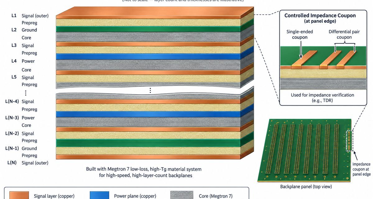
A Megtron 7 PCB stackup must be frozen as an electrical and manufacturing contract before layer count or impedance changes are approved. High-layer-count digital boards rarely fail because an engineer forgot to draw a trace. They fail when a late layer move changes dielectric thickness, resin distribution, or reference-plane continuity and the impedance model is...
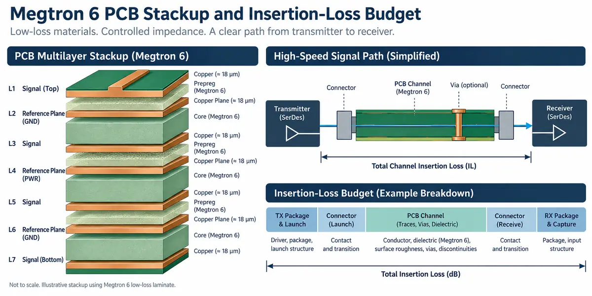
Megtron 6 PCB for 112G Backplanes: Managing Skew, Vias, and Reference-Plane Continuity

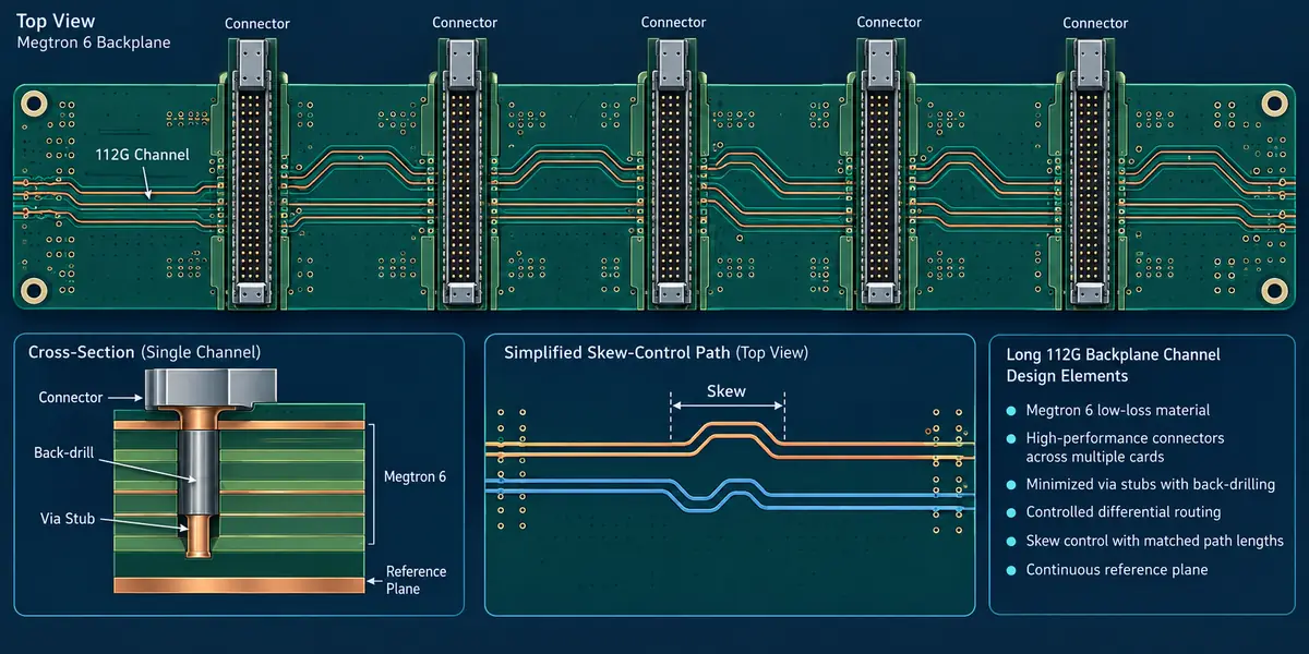
Table of Contents Channel construction Skew and weave control Via and plane continuity Coupon and release checks The released Megtron 6 PCB stackup must keep the 112G lane assumptions visible to design and fabrication. At this data rate, a small skew shift, a poorly referenced via field, or a connector launch that changes between panels...

Megtron 6 PCB Material Selection: Turning Loss Budgets into a Manufacturable Stackup

Megtron 6 PCB projects often fail late for a simple reason: the electrical loss budget was written before the stackup, copper profile, and connector geometry were frozen. A material family can support demanding high-speed channels, but the released board still depends on resin content, finished dielectric thickness, reference-plane continuity, copper roughness, and fabrication capability. This...

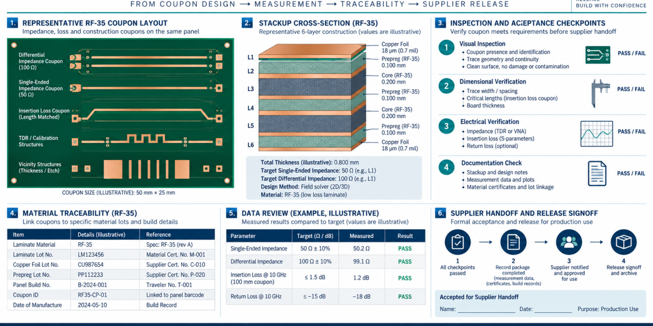
Taconic RF-35 PCB Coupon Design: Correlating Stackup, Impedance, and Production Release

Table of Contents Coupon decision and field geometry Measurement interface Data interpretation Production release gate An impedance coupon is valuable only when it represents the product path that the project team is trying to release. For a Taconic RF-35 PCB, a generic straight-line coupon may confirm a number while hiding the real risk in a...

Multilayer PCB: Advanced Design for High-Density and High-Speed Electronics

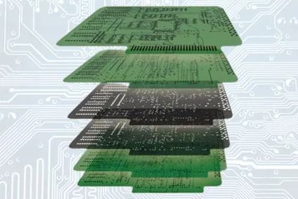
Multilayer PCB: Advanced Design for High-Density and High-Speed Electronics With modern electronic devices becoming increasingly compact and high-performance, Multilayer PCB technology is essential for achieving complex circuit routing, improved signal integrity, and efficient power distribution. A multilayer PCB consists of three or more conductive copper layers laminated together with dielectric materials , enabling compact, high-density,...

Multilayer PCB: Structure, Benefits, and Applications in Modern Electronics

What Is a Multilayer PCB? A multilayer PCB is a printed circuit board composed of multiple copper layers separated by prepreg and core materials. Unlike single-sided or double-sided PCBs, multilayer boards provide additional routing layers, allowing engineers to design high-density circuits with improved electrical performance. Typical multilayer PCB configurations include: 4-layer PCB 6-layer PCB 8-layer...

Rogers PCB: Low Loss High Frequency PCB Solutions for RF and Microwave Applications

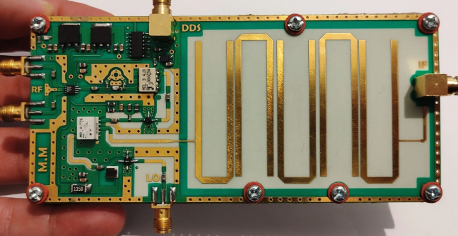
A Rogers PCB is a high-performance printed circuit board manufactured using Rogers high-frequency laminate materials, which outperform standard FR-4 in RF, microwave, and high-frequency signal applications. Rogers PCB materials provide low dielectric loss, stable dielectric constant (Dk), and excellent controlled impedance, making them essential for modern high-speed electronics and wireless communication systems. As technology evolves,...

High Speed PCB Engineering for Signal Integrity, Power Integrity, and Ultra-Low-Latency Electronic Systems

As modern electronics become faster, more compact, and more data-intensive, the High Speed PCB has evolved into a critical engineering platform for communication systems, servers, AI accelerators, radar units, embedded computing modules, and advanced industrial electronics. A well-engineered High Speed PCB ensures clean signal transmission, stable power behavior, and low-jitter operation across multi-gigabit channels. High-speed...

Engineering High Speed PCB for Signal Integrity, Low-Loss Routing, and Next-Generation Data Transmission

As digital systems move toward higher data rates, smaller form factors, and lower power consumption, the demand for High Speed PCB solutions continues to accelerate. From 10–112 Gbps SerDes links to DDR4/DDR5 memory buses and advanced communication modules, a High Speed PCB must deliver loss control, impedance stability, and electromagnetic reliability in increasingly complex environments....

High Speed PCB Engineering Strategies for Ultra-Reliable, High-Bandwidth, Next-Generation Electronic Systems

A High Speed PCB is no longer a specialty board reserved for telecom giants—it has become the core platform for every high-bandwidth, low-latency, high-frequency electronic architecture. Whether powering 56G/112G SerDes, PCIe 5.0/6.0 interconnects, next-generation routers, AI accelerator hardware, or advanced radar/5G infrastructure, the High Speed PCB defines the system’s ultimate signal integrity, timing accuracy, power...