
Table of Contents
- Coupon decision and field geometry
- Measurement interface
- Data interpretation
- Production release gate
An impedance coupon is valuable only when it represents the product path that the project team is trying to release. For a Taconic RF-35 PCB, a generic straight-line coupon may confirm a number while hiding the real risk in a connector launch, via transition, coupled line, or mixed dielectric stackup. Coupon design should therefore begin with the release question, not with a convenient spare area on the panel.
Start with the Taconic RF-35 PCB decision the coupon must support
Before placing a coupon, define what the result will approve: a single-ended feed, differential pair, coupled-line filter, RF via, connector launch, or the complete stackup. Record the target impedance, frequency band, trace class, and measurement method. If the project will use a VNA, state the calibration reference plane and fixture interface. If the result is only for process correlation, do not present it as an in-product measurement.
A Taconic RF-35 PCB coupon should mirror the finished dielectric height, copper condition, solder-mask state, and reference-plane geometry of the critical net. Public RF-35 supplier data, such as typical Dk near 3.50 and Df near 0.0018 at a specified test frequency, can support the initial model. The coupon still has to prove the finished construction that the supplier actually builds.
| Coupon question | Representative feature | Release evidence |
|---|---|---|
| Is the line impedance controlled? | Finished trace width and dielectric height | Cross-section plus impedance result |
| Is the launch repeatable? | Connector pad, antipad, and ground fence | Launch coupon or transition structure |
| Is the stackup correlated? | Same layer pair and copper condition | Stackup revision and material lot |
| Can production trace the result? | Panel and coupon identification | Lot, panel, and measurement record |
Mirror the field geometry, not only the nominal width
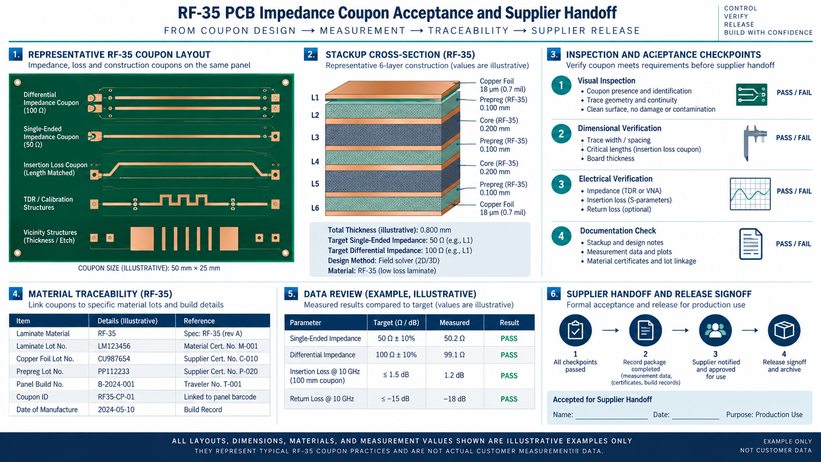
The most common Taconic RF-35 PCB coupon mistake is to copy the trace width while changing the environment around it. A product line may have a nearby ground via, a cutout, a solder-mask opening, a connector pad, or a copper pour edge that the coupon omits. Those differences change the effective impedance and the return current.
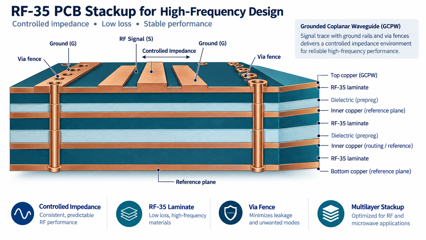
Use the same layer assignment for a Taconic RF-35 PCB and reference-plane spacing as the product path. For a controlled-impedance PCB, show the trace, side grounds, via fence, and plane openings in the coupon drawing. If the product uses a layer transition, include the transition rather than trying to infer its behavior from a long uniform trace.
A Taconic RF-35 PCB coupon can include both a launch structure and a uniform line. The uniform line helps correlate the stackup; the launch structure exposes the discontinuity that the system will actually see. Keep the two results separate in the report so a good line does not mask a poor launch.
Choose a measurement interface the factory can repeat
Probe pads on a Taconic RF-35 PCB, edge launches, and coax connectors each have a different error budget. A probe coupon needs pad pitch, ground clearance, and probe contact repeatability. An edge-launch coupon needs a controlled board edge, connector seating, and a documented torque or fixture method. A connectorized structure should identify the connector part, launch drawing, and de-embedding reference.
For first articles, include a short setup checklist: calibration kit, cable routing, fixture ID, ambient condition, and operator sign-off. These details do not turn the coupon into a customer test report; they make the result reproducible when the next panel is measured.
Interpret coupon data without overclaiming
Separate typical Taconic RF-35 PCB supplier values, design targets, and measured values in the release package. A typical Dk or Df is a material reference. A target impedance is a design requirement. A measured coupon result belongs to one panel, one stackup revision, and one test method. Mixing those categories is how a project team ends up arguing over a number that was never comparable.
When a result is outside the window, compare the finished cross-section first: trace width, copper thickness, dielectric height, mask condition, and plane clearance. Then review the fixture and calibration reference. Only after those checks should the team consider a material or stackup change. This sequence protects both schedule and engineering credibility.
Build a release package that survives procurement
KKPCB’s impedance coupon review should link the coupon drawing to the stackup, drill file, panel map, and inspection plan. Put the coupon ID in the fabrication notes and require the supplier to return the measured result with the panel or lot ID. If the build combines RF and digital layers, identify the RF coupon separately from the digital test structure.
A PCB manufacturing handoff for a Taconic RF-35 PCB should also state how substitutions are handled. If copper foil, resin content, or dielectric thickness changes, the coupon model and acceptance window may need to be reissued. That simple rule prevents a “same material” substitution from silently changing the RF path.
Use the coupon as a project gate
A useful Taconic RF-35 PCB gate asks whether the coupon mirrors the product geometry, whether its measurement interface is repeatable, whether the result is traceable to a panel, and whether the acceptance window is tied to system margin. A Taconic RF-35 PCB release that answers those questions gives design, sourcing, manufacturing, and test teams the same evidence.
For purchasing and test teams, pair the release with an RF test coupon record and a PCB stackup revision note.
Sources: public RF-35 supplier data for typical electrical properties; Analog Devices guidance on controlled impedance and RF measurement structures; KKPCB coupon, stackup, and production-release workflow information reviewed for this article.
