PCB layout - KKPCB
 
HomeTag

PCB layout - KKPCB

Printed Circuit Boards with Embedded Components: From Concept to Production

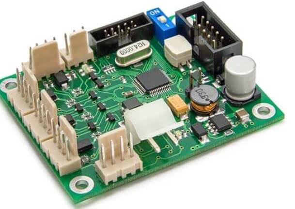
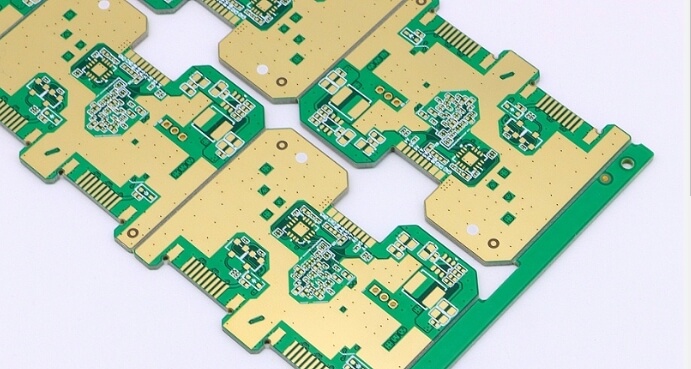
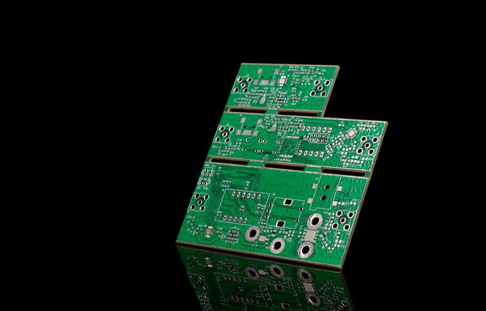
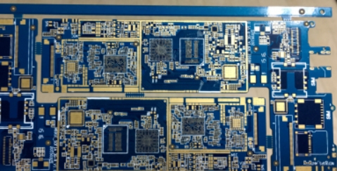
Looking back and examining the evolution of computing technology, we see that many products widely used in everyday life today have changed significantly over time. Looking back at Apollo workstations, the first PCs, and mainframes that could occupy entire floors of buildings, it becomes clear that miniaturization has been the foundation of technological progress. Recent...

PCB Layout Best Practices: Essential Design Considerations for Reliable Electronic Products

PCB design translates electrical schematics into a functional product, and its quality directly impacts production efficiency and product reliability. For beginners, mastering PCB layout can be challenging despite familiarity with design software, and common issues often arise. Here, seasoned engineers from KKPCB share their PCB layout insights to help avoid these pitfalls and inspire best practices. Component Placement...

What are Thin and Thick Film Resistors?

Thin and Thick Film Resistors are the most common types in the market. They are characterized by a resistive layer on a ceramic base. Although their appearance might be very similar, their properties and manufacturing process are very different. The naming originates form the different layer thicknesses. Thin film has a thickness in the order of 0.1μm...

The Five Golden Rules of PCB Design

Printed Circuit Board (PCB) design is a critical step in the development of any electronic product. A well-designed PCB ensures reliability, performance, and manufacturability, while a poor design can lead to costly failures and delays. Below are five golden rules that every PCB designer should follow. 1. Prioritize Clear and Logical Layout A clean and...

Grounding method in multilayer PCB circuit board

In modern multilayer PCB circuit board design, selecting the correct grounding method is essential for ensuring optimal signal integrity, minimizing electromagnetic interference (EMI), and maintaining stable power integrity. A well-designed grounding system not only improves overall PCB performance but also enhances the reliability of high-speed and high-frequency electronic applications. One of the most widely used...

Blind Via and Buried Via

In modern PCB design, Blind Via and Buried Via technologies play a critical role in achieving high-density interconnect (HDI) structures, improving signal integrity, and optimizing PCB layout performance. As electronic devices continue to evolve toward miniaturization, high speed, and high functionality, the use of blind vias and buried vias has become increasingly essential in advanced...

PCB Resistors and Board Design

In modern electronics, PCB resistors play a vital role in ensuring circuit stability, signal control, and power regulation. Whether in rigid circuit boards, multilayer PCBs, or advanced PCBA designs, proper resistor selection and placement are crucial for achieving optimal performance. Understanding how resistors in PCB design interact with layout and signal behavior is key to...