PCB Design - KKPCB
 
HomeTag

PCB Design - KKPCB

Taconic TLY-5 PCB Material: A Complete Technical Guide for High-Frequency, RF, and Microwave Applications

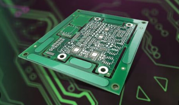
The Role of TLY-5 in High-Frequency PCBs Taconic TLY-5 PCB material is a PTFE-based high-frequency laminate designed to meet the demanding requirements of RF, microwave, and high-speed PCB applications. Its low dielectric loss, stable dielectric constant, and excellent thermal and mechanical properties make it a top choice for wireless communication systems, industrial wireless sensor networks...

Single Layer PCBs: A Complete Technical Guide to Structure, Design Rules, Manufacturing Processes, and Applications

Why Single Layer PCBs Still Matter Although modern electronics are increasingly dominated by multilayer PCBs, HDI structures, and high-frequency RF boards, single layer PCBs (Single-Sided PCBs) remain widely used due to their low cost, simple design, and high manufacturability. Single layer PCBs are still essential in: Cost-sensitive electronic products Simple analog circuits Power control modules...

Advancing Dielectric Uniformity and RF Efficiency of Taconic TLY-5 PCB Laminates for Industrial Wireless Sensor Networks

Enabling High-Performance Industrial Wireless Networks In industrial wireless sensor networks (IWSNs), PCB materials play a critical role in achieving reliable communication and efficient signal transmission. Taconic TLY-5 PCB laminates are engineered for high-frequency applications, offering exceptional dielectric uniformity, low dissipation factor, and excellent RF performance, making them ideal for industrial IoT and wireless sensor networks....

PCB Design Guidelines for EMC Compliance

Why EMC Matters in PCB Design Electromagnetic Compatibility (EMC) is a key requirement in modern PCB design, ensuring that electronic systems operate reliably without generating or being affected by electromagnetic interference (EMI). Proper PCB layout—especially GND routing, trace spacing, and layer design—plays a decisive role in reducing ESD (Electrostatic Discharge) and improving overall signal integrity....

Why Should Vias Be Staggered from Pad Positions in PCB Design?

 The Importance of Via Placement in PCB Design In PCB design, via positioning plays a crucial role in ensuring electrical performance, manufacturing reliability, and signal integrity. Improper via placement—especially placing vias directly on component pads—can lead to soldering defects, electrical noise, and higher production costs. This article explains why vias should be staggered from pad...

PCBs for Industrial Automation: The Backbone of Modern Control Systems

In the era of Industry 4.0, industrial automation systems rely heavily on high-performance printed circuit boards (PCBs) to enable intelligent control, real-time data processing, and reliable system operation. As the backbone of modern control systems, industrial automation PCBs must deliver exceptional reliability, durability, and electrical stability. From programmable logic controllers (PLCs) to robotics and smart...

Mastering High-Speed PCB Test Point Design: Precision, Performance, and Signal Integrity

Mastering High-Speed PCB Test Point Design: Precision, Performance, and Signal Integrity In high-speed printed circuit board (PCB) design, test point placement is far more than a routine step—it’s a science of balance. The miniature metal pads scattered across a PCB may look simple, but their position, size, and electrical behavior can determine whether a product...

Explore how KKPCB engineers world-class radar PCBs for automotive, aerospace, and defense applications. Learn about design techniques, RF materials, and manufacturing precision for frequencies up to 77 GHz.

Radar PCB Overview Radar PCBs represent the pinnacle of high-frequency circuit design, bridging advanced RF engineering and precise manufacturing. These specialized boards operate in the 1 GHz – 77 GHz range, demanding exceptional signal integrity, low loss materials, and extreme reliability — especially in mission-critical applications like automotive radar, aerospace, and defense. KKPCB has extensive...

PCB Design Best Practices: Key Considerations for Optimized Performance

When designing printed circuit boards (PCBs), a well-structured approach and attention to detail are essential to ensure functionality and avoid potential design errors. Here are some key PCB design tips based on practical experience: 1. Pay Attention to Pin Definitions and Package Names in the Schematic Library When creating the schematic library, ensure that each schematic pin corresponds correctly...