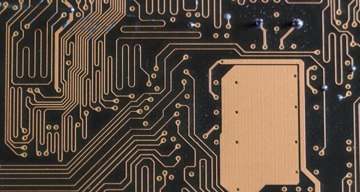
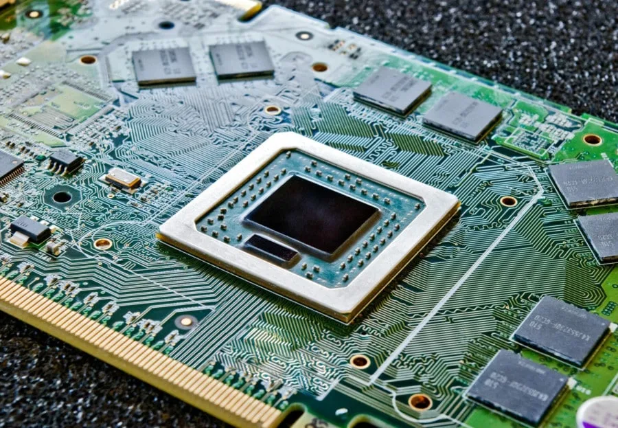
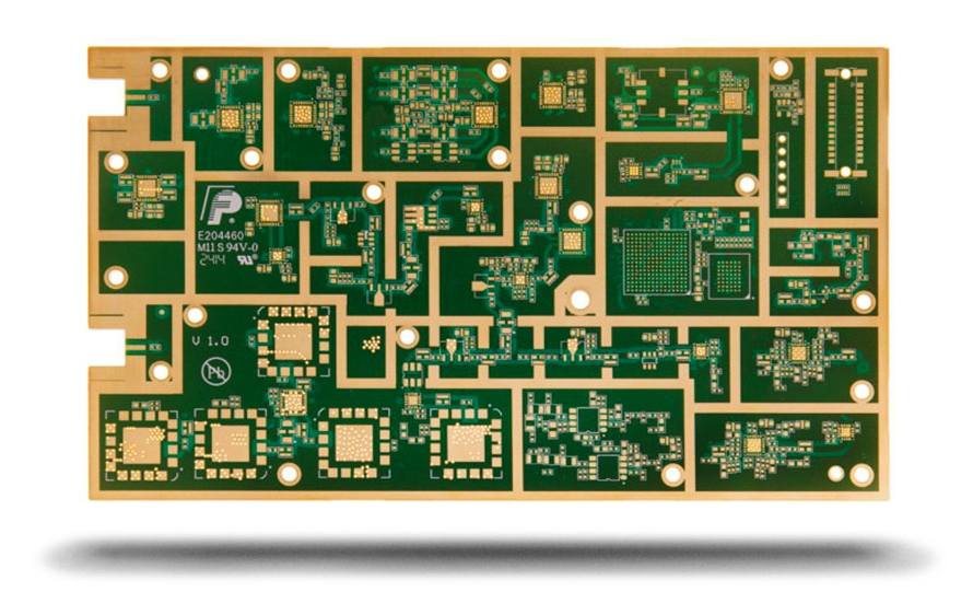
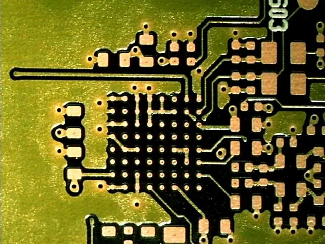
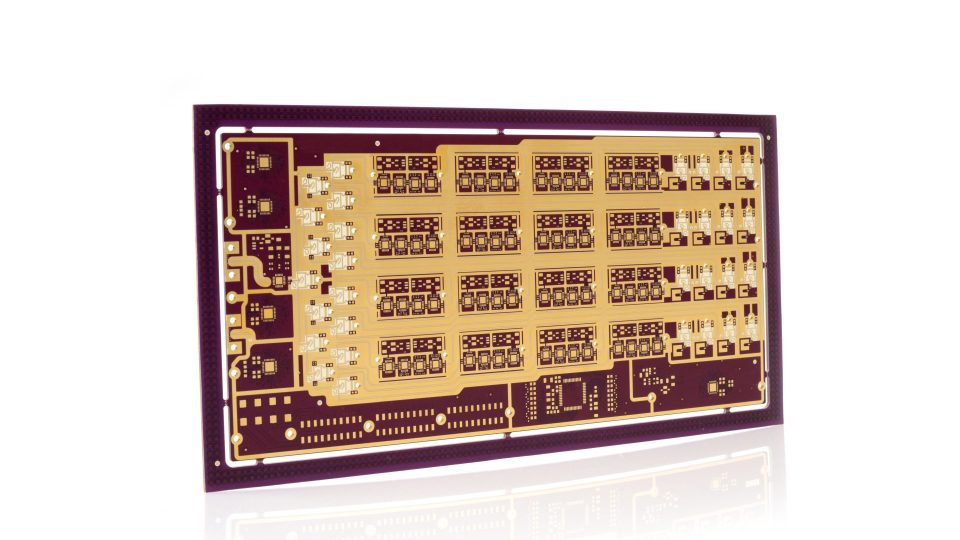
Microvia PCB - KKPCB
 
HomeTag

Microvia PCB - KKPCB

Fine Line PCB: High-Density, Precision PCB Solutions for Advanced Electronics

What Is a Fine Line PCB? A Fine Line PCB is a printed circuit board engineered with ultra-narrow traces and tight spacing, typically below 100 µm. This enables high-density routing and compact component placement while maintaining excellent signal integrity and reliability. Fine line PCBs are essential in high-speed digital systems, RF modules, 5G devices, IoT...

Microvia PCB: Enabling HDI, Miniaturization, and High-Speed Electronic Design

A Microvia PCB is an advanced printed circuit board technology specifically developed for HDI PCB (High Density Interconnect PCB) and high-density PCB applications. By utilizing laser-drilled microvias, Microvia PCBs enable extremely compact routing, superior signal integrity, and reliable interconnections in modern high-speed and high-frequency electronic systems. As electronic products continue to evolve toward miniaturization, higher...

High Reliability PCB: Robust PCB Solutions for Mission-Critical Electronics

A High Reliability PCB is a printed circuit board engineered to maintain consistent electrical and mechanical performance over extended service life, even under harsh environmental and operational conditions. Unlike standard PCBs, high reliability PCBs are designed with enhanced materials, robust structures, and stringent manufacturing controls to meet the demands of mission-critical applications. As electronics are...

Multilayer PCB: Advanced PCB Solutions for High-Density and High-Performance Electronics

A Multilayer PCB is a printed circuit board composed of three or more conductive copper layers laminated together with insulating dielectric materials. Compared to single-layer and double-layer boards, multilayer PCBs offer higher routing density, improved electrical performance, and greater design flexibility, making them essential for modern electronic products. As electronic systems continue to evolve toward...

Low Loss PCB: Advanced PCB Technology for High-Speed, RF, and High-Frequency Applications

A Low Loss PCB is a specialized printed circuit board designed to reduce dielectric loss, insertion loss, and signal distortion in high-speed and high-frequency electronic systems. As modern electronics such as 5G communication systems, RF front-end modules, high-speed data transmission, and semiconductor test equipment operate at ever-increasing frequencies, signal integrity becomes a critical design challenge....

Microvia PCB: The Ultimate Solution for HDI and High-Speed PCB Designs

In today’s rapidly evolving electronics market, devices are becoming smaller, faster, and more complex. To meet these demands, Microvia PCBs have become a critical solution in HDI PCB and high-speed PCB design. Microvias are extremely small vias that create precise interlayer connections, allowing for high-density routing, improved signal integrity, and reliable performance in modern electronic...

Multilayer PCB: Advanced Solutions for High-Density and High-Performance Electronics

A Multilayer PCB is a printed circuit board composed of three or more layers of conductive traces separated by insulating substrates, allowing more complex circuitry, higher routing density, and superior signal integrity. Multilayer PCBs are widely used in high-speed computing, RF communication, IoT, semiconductor testing, and automotive systems, where compact size and high performance are...

Low Loss PCB: High-Performance Solutions for RF, 5G, and High-Speed Electronics

A Low Loss PCB is a specialized printed circuit board engineered to minimize signal attenuation, dielectric loss, and crosstalk in high-speed, high-frequency, and RF electronic systems. With the rise of 5G, IoT, high-speed computing, and advanced semiconductor testing, ensuring signal integrity and reliable performance is more critical than ever. Key Features of Low Loss PCBs...

Fine Pitch PCB: Precision Solutions for High Pin Count and Miniaturized Electronics

A Fine Pitch PCB is a printed circuit board designed to support high-density integrated circuits with extremely small pad spacing, such as BGA, QFN, CSP, and flip-chip packages. As modern electronics continue to shrink in size while increasing functionality, fine pitch PCB technology becomes essential for achieving high routing density, reliable assembly, and superior electrical...

High Density PCB: Advanced Solutions for Compact and High-Performance Electronics

A High Density PCB (HDPCB) is a printed circuit board designed to support compact, high-performance electronic systems. By leveraging HDI technology, microvias, blind/buried vias, and multilayer stackups, high density PCBs allow engineers to integrate more functionality into smaller footprints, making them essential for smart devices, high-speed computing, RF communication, and semiconductor testing. Key Features of...