
The Growing Importance of Fine Pitch PCB Technology
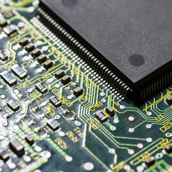
As electronic devices continue to become smaller, faster, and more functionally complex, traditional PCB structures face increasing limitations in supporting high-density components and advanced semiconductor packages.
A Fine Pitch PCB is specifically designed to support components with extremely small pin spacing and high I/O density, including:
- BGA (Ball Grid Array)
- QFN (Quad Flat No-lead Package)
- CSP (Chip Scale Package)
- Flip-chip packages
- Advanced semiconductor devices
By combining ultra-fine routing, microvia technology, and advanced multilayer structures, fine pitch PCBs enable compact electronic designs while maintaining reliable signal transmission, power integrity, and assembly performance.
What Is a Fine Pitch PCB?
A Fine Pitch PCB is a high-density printed circuit board manufactured with narrow trace widths, tight spacing, and advanced interconnection technologies to accommodate modern high-pin-count components.
Unlike conventional PCBs, fine pitch PCBs focus on:
- Maximizing routing density
- Supporting miniature semiconductor packages
- Maintaining signal integrity at high speeds
- Improving assembly reliability
These capabilities make fine pitch PCB technology essential for applications where size, performance, and reliability are equally critical.
Key Features of Fine Pitch PCBs
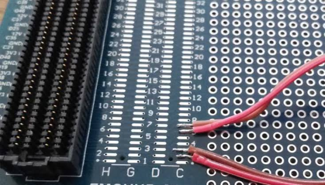
1. Ultra-Fine Line and Space Technology
One of the defining characteristics of fine pitch PCBs is their ability to support extremely narrow conductor geometries.
Advanced manufacturing processes enable:
- Fine line widths and spacing down to 3 mil or below
- High-density routing between small pads
- Reduced PCB size without sacrificing functionality
Precise etching and registration control are essential to maintain electrical consistency and production yield.
2. Microvia and Via-in-Pad Technology
Fine pitch components require advanced via structures to escape dense pad layouts.
Microvia and via-in-pad technologies provide significant advantages:
- Shorter signal paths
- Reduced parasitic inductance
- Improved high-speed signal integrity
- More efficient fan-out routing
These technologies are particularly important for:
- High-speed digital circuits
- RF modules
- Semiconductor test boards
- Advanced computing platforms
3. Advanced Multilayer Stackup Design
Fine pitch PCBs typically utilize multilayer structures to support complex routing requirements.
Optimized stackups provide:
- Dedicated power and ground planes
- Controlled impedance performance
- Improved EMI suppression
- Better thermal distribution
Proper layer planning ensures reliable electrical performance even in highly integrated designs.
4. High Pin Count and Advanced Package Support
Modern semiconductor packages continue to increase in I/O density, creating greater challenges for PCB routing.
Fine pitch PCBs are designed to support:
- High-density BGA packages
- Fine-pitch QFN components
- CSP and advanced IC packages
- Multi-chip modules
Advanced breakout strategies and HDI structures allow engineers to achieve compact layouts while maintaining manufacturing reliability.
5. Signal Integrity and Electrical Performance
As signal speeds increase, PCB layout precision becomes increasingly important.
Fine pitch PCB designs help maintain electrical performance through:
- Controlled impedance routing
- Optimized return paths
- Reduced via parasitics
- Improved power distribution networks (PDN)
These features minimize:
- Signal reflection
- Crosstalk
- Timing errors
- Electromagnetic interference
6. Thermal and Mechanical Reliability
High-density electronic systems generate more heat within smaller spaces.
Reliable fine pitch PCBs require:
- Stable laminate materials
- Controlled thermal expansion
- Robust via structures
- Reliable copper plating
These factors help prevent:
- Layer delamination
- Via cracking
- Mechanical deformation
- Long-term reliability issues
Applications of Fine Pitch PCBs
Fine pitch PCB technology is widely used in industries requiring compact, high-performance electronic systems.
Semiconductor and IC Testing
Fine pitch PCBs are commonly used in:
- IC test boards
- Load boards
- Package test boards
- Burn-in boards
They provide the high-density routing and signal accuracy required for semiconductor validation.
Communication and RF Systems
Applications include:
- 5G communication modules
- RF front-end circuits
- High-frequency devices
- Antenna systems
Fine pitch structures help maintain signal integrity in compact RF designs.
Automotive Electronics
Modern vehicles rely on high-density electronics for:
- ADAS systems
- Automotive controllers
- Sensor modules
- Electric vehicle systems
Fine pitch PCBs support advanced functionality while meeting reliability requirements under harsh environments.
Medical and Industrial Electronics
Compact and reliable PCB solutions are essential for:
- Medical devices
- Industrial control systems
- Smart sensors
- IoT equipment
Fine pitch PCB technology enables smaller designs without compromising performance.
Manufacturing Challenges of Fine Pitch PCBs
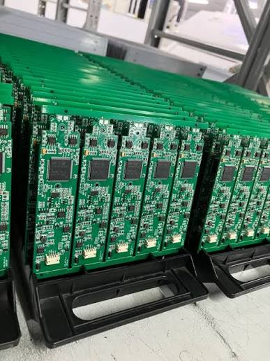
Producing reliable fine pitch PCBs requires advanced fabrication capabilities.
Precision Manufacturing Requirements Include:
High-Accuracy Laser Drilling
Microvia formation requires:
- Precise laser drilling control
- Reliable via plating
- Stable hole dimensions
Fine-Line Etching Control
Maintaining narrow traces requires:
- Accurate imaging technology
- Controlled etching processes
- Tight registration tolerance
Via Filling and HDI Processing
Advanced structures such as via-in-pad require:
- Copper filling technology
- Void control
- Reliable plating processes
Inspection and Quality Control
Fine pitch PCB production requires comprehensive inspection, including:
- AOI inspection
- X-ray inspection
- Electrical testing
- Impedance verification
These processes ensure consistent quality and high production yield.
Choosing the Right Fine Pitch PCB Manufacturing Partner
A capable fine pitch PCB manufacturer should provide:
- HDI PCB manufacturing experience
- Microvia and via-in-pad capability
- High-layer multilayer fabrication
- Controlled impedance technology
- Prototype and volume production support
- Engineering assistance for DFM optimization
Early engineering collaboration helps identify manufacturability risks and improves production success.
Conclusion
Fine Pitch PCB technology plays a critical role in enabling next-generation electronic systems that demand higher integration, smaller form factors, and faster signal performance.
Through advanced HDI structures, microvia technology, precision manufacturing, and optimized stackup design, fine pitch PCBs provide the foundation for reliable high-density electronics.
From semiconductor testing and communication systems to automotive and industrial applications, selecting an experienced fine pitch PCB manufacturer ensures better electrical performance, higher production yield, and long-term product reliability.
