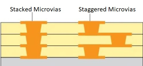
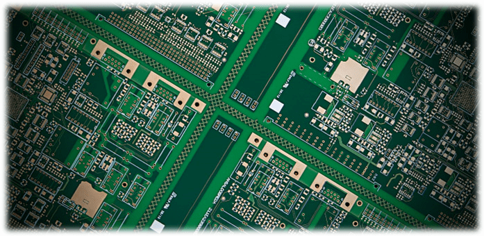
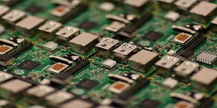
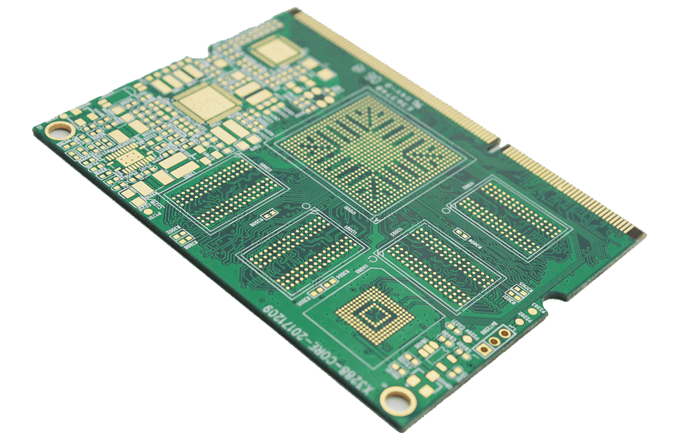
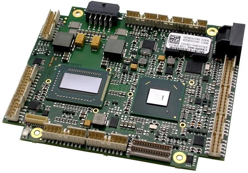
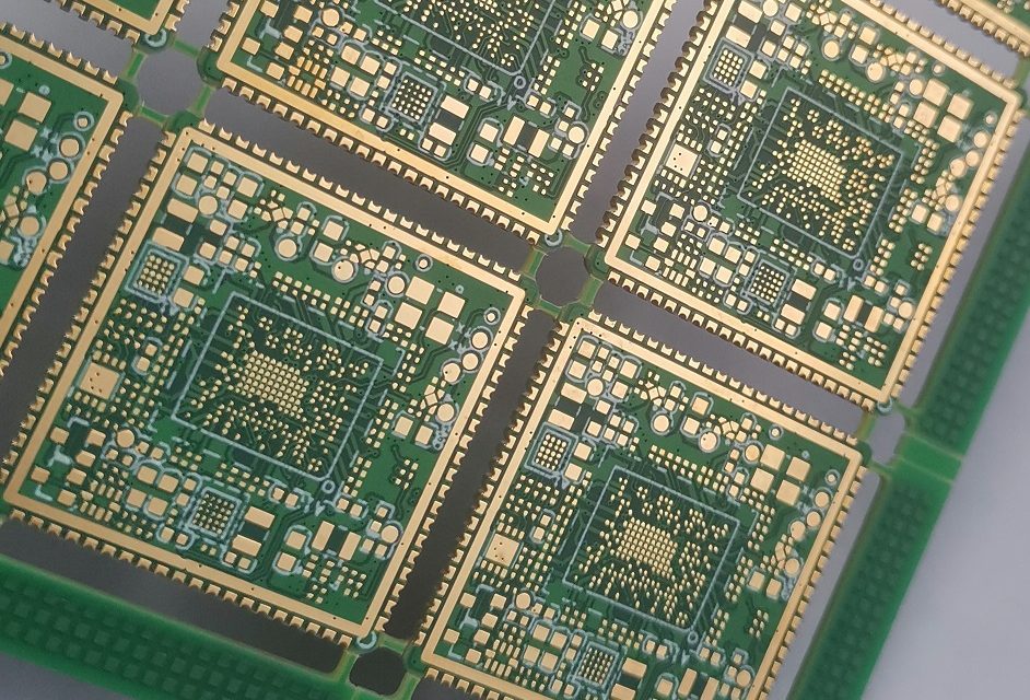
Microvia PCB - KKPCB
 
HomeTag

Microvia PCB - KKPCB

Microvia PCB Technology for HDI, High-Speed, and Miniaturized Electronic Systems

What Is a Microvia PCB? A Microvia PCB is an advanced type of HDI (High Density Interconnect) printed circuit board that uses laser-drilled microvias, typically with a diameter of ≤150 μm, to interconnect PCB layers. Unlike traditional mechanical vias, microvias are designed for shorter signal paths, higher routing density, and compact layouts, making them essential...

Multilayer PCB: Enabling High-Density, High-Speed, and Complex Electronic Systems

A Multilayer PCB is a printed circuit board composed of three or more conductive copper layers laminated together with insulating materials. As electronic products continue to demand higher functionality, faster signal speeds, and smaller form factors, multilayer PCBs have become the backbone of advanced electronics, semiconductor testing, communication systems, and industrial control equipment. Compared with...

Low Loss PCB: High-Performance Solutions for High-Speed and High-Frequency Electronics

A Low Loss PCB is a specialized printed circuit board designed to minimize signal attenuation, dielectric loss, and insertion loss in high-speed digital and high-frequency RF applications. As modern electronics operate at multi-GHz frequencies and multi-gigabit data rates, signal loss caused by PCB materials and structures becomes a critical limiting factor. Low loss PCBs are...

Fine Pitch PCB: Precision Manufacturing for High Pin Count and Miniaturized Electronics

A Fine Pitch PCB is a printed circuit board specifically designed to support high pin count ICs and ultra-small component spacing, commonly found in modern semiconductor devices, high-speed electronics, IoT modules, automotive electronics, and advanced test boards. As electronic products continue to shrink while integrating more functions, fine pitch PCB technology has become essential for...

High Density PCB: Advanced Design and Manufacturing for Compact and High-Performance Electronics

A High Density PCB (HDPCB) is a specialized printed circuit board designed for compact, high-performance, and high-pin-count electronic applications. HD PCBs are widely used in semiconductor test boards, IoT devices, wearable electronics, automotive systems, and high-speed communication modules, where space constraints, signal integrity, and reliability are critical. High density PCBs combine fine-pitch component layouts, multilayer...

IoT IC Test PCB: Precision Test Solutions for Low-Power and Connected Devices

An IoT IC Test PCB is a specialized printed circuit board designed to validate low-power, high-density, and high-functionality IoT integrated circuits. These ICs combine analog, digital, RF, and sensor interfaces in compact packages, often operating at low voltages and requiring precise timing for wireless communication. IoT IC test PCBs are widely used in Automated Test...

Automotive IC Test PCB: Reliable Test Solutions for Automotive-Grade Integrated Circuits

An Automotive IC Test PCB is a specialized printed circuit board used to validate automotive-grade integrated circuits, including power management ICs, microcontrollers, ADAS sensors, RF modules, and in-vehicle communication ICs. Automotive ICs must meet stringent reliability standards due to harsh operating environments, temperature extremes, and safety-critical applications. These test PCBs play a critical role in...

HDI PCB: High-Density Interconnect Technology for Compact and High-Speed Electronic Designs

As electronic products continue to evolve toward smaller form factors and higher performance, conventional PCB technologies often reach their limits. The HDI PCB (High-Density Interconnect PCB) overcomes these limitations by enabling ultra-dense routing, shorter signal paths, and enhanced electrical performance. A professionally engineered HDI PCB is essential for modern high-speed and high-density electronic systems. What...

HDI PCB: Advanced High-Density Interconnect Solutions for Compact and High-Speed Electronics

As electronic devices become smaller, faster, and more complex, traditional PCB technologies often struggle to meet space and performance requirements. The HDI PCB (High-Density Interconnect PCB) addresses these challenges by enabling ultra-dense routing, shorter signal paths, and improved electrical performance in compact form factors. A professionally designed HDI PCB is essential for modern high-speed, high-pin-count,...

HDI PCB: Advanced Interconnect Technology for Compact, High-Performance Electronics

As electronic devices become smaller, faster, and more complex, traditional PCB technologies often reach their physical limits. HDI PCB (High Density Interconnect PCB) technology was developed to overcome these challenges by enabling higher wiring density, finer geometries, and improved electrical performance. A professionally manufactured HDI PCB is a key enabler for modern consumer electronics, communication...