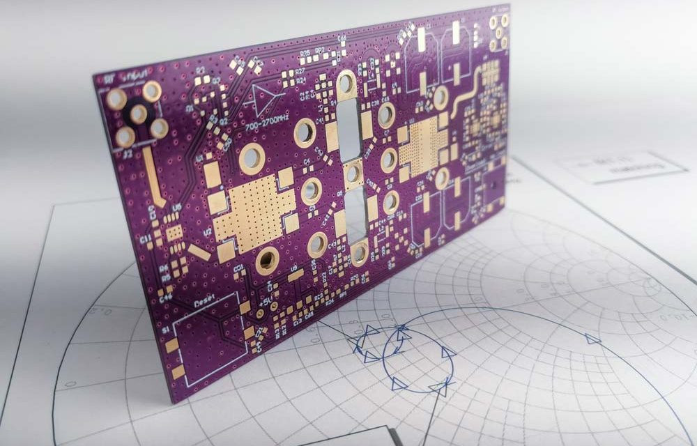
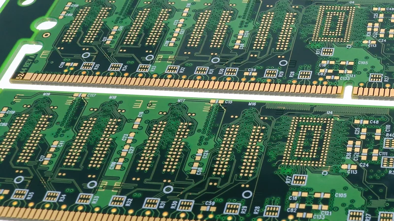
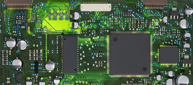
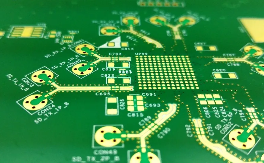
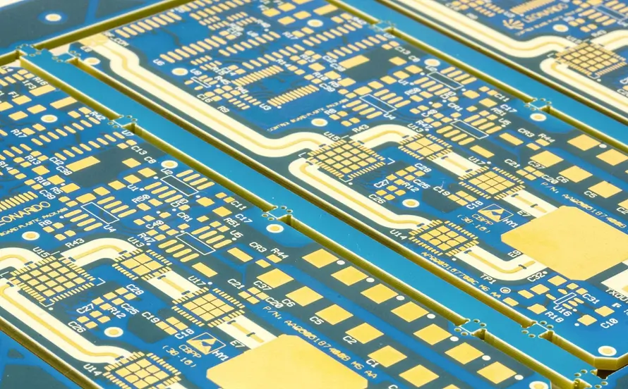
Microvia PCB - KKPCB
 
HomeTag

Microvia PCB - KKPCB

High Frequency Signal PCB Manufacturing for High-Speed and RF Applications

What Is a High Frequency Signal PCB? A High Frequency Signal PCB is a printed circuit board designed to carry high-speed and high-frequency signals with minimal loss, reflection, or distortion. These PCBs are crucial in RF, microwave, 5G, high-speed computing, and semiconductor test applications, where signal integrity and low insertion loss are essential for system...

RF Trace PCB Manufacturing for High-Frequency and Wireless Applications

What Is an RF Trace PCB? An RF Trace PCB is a printed circuit board designed to route high-frequency RF signals with minimal signal loss, reflection, and distortion. These PCBs are optimized for controlled impedance, low insertion loss, and high signal integrity, making them essential for applications such as 5G modules, mmWave systems, wireless communication,...

Fine Line PCB Manufacturing for High-Density and High-Performance Electronics

What Is a Fine Line PCB? A Fine Line PCB is a printed circuit board that uses extremely narrow traces and spaces to support high-density, complex electronic designs. Fine line technology is essential for applications where board real estate is limited but high-speed performance and signal integrity are required, such as smartphones, 5G modules, high-speed...

Microvia PCB Manufacturing for High Density and High Performance Electronics

What Is a Microvia PCB? A Microvia PCB is a printed circuit board that uses microvias, which are very small drilled holes (typically <150 μm) to interconnect layers in high-density, multilayer HDI PCBs. Microvias enable fine-pitch routing, high pin count IC integration, and compact board layouts, making them essential for advanced electronics such as smartphones,...

HDI PCB: High Density Interconnect PCB Manufacturing for Advanced Electronic Applications

An HDI PCB (High Density Interconnect PCB) is a key technology enabling compact, lightweight, and high-performance electronic products. As electronic devices continue to evolve toward smaller form factors, higher functionality, and faster data transmission, traditional PCB designs can no longer meet density and routing requirements. HDI PCB technology provides higher wiring density per unit area...

Fine Line PCB: High Precision PCB Manufacturing for HDI and High-Density Routing

What Is a Fine Line PCB? A Fine Line PCB is a high-precision printed circuit board manufactured with ultra-thin trace width and tight trace spacing, enabling high-density routing for advanced electronic products. Compared with standard PCB technology, Fine Line PCB fabrication focuses on achieving smaller line/space (L/S), higher wiring density, and improved signal performance in...

High Frequency Signal PCB: Ensuring Optimal Performance for High-Speed Electronics

What Is a High Frequency Signal PCB? A High Frequency Signal PCB is a printed circuit board specifically engineered to handle high-speed and high-frequency signals with minimal signal loss and optimal signal integrity. These PCBs are crucial in RF communication, 5G modules, high-speed computing, IoT devices, and automotive radar systems. High frequency signals require careful...

Fine Line PCB: Precision Routing for High-Density and High-Speed Electronics

What Is a Fine Line PCB? A Fine Line PCB is a printed circuit board designed with ultra-thin traces and narrow spacing, typically under 4 mils (0.1 mm), enabling high-density interconnections for compact electronic devices. Fine line PCBs are essential in applications where space constraints, high-speed signals, and precise routing are required, such as 5G...

Signal Integrity PCB Design for High-Speed and High-Frequency Electronics

What Is a Signal Integrity PCB? A Signal Integrity PCB is a printed circuit board specifically designed to preserve the quality, timing, and accuracy of electrical signals as they propagate through high-speed and high-frequency circuits. As signal speeds increase and edge rates become faster, maintaining signal integrity (SI) becomes a critical factor in overall system...

Microvia PCB: Advanced HDI PCB Technology for Miniaturized and High-Performance Electronics

Introduction to Microvia PCB A Microvia PCB is a key enabling technology in HDI (High Density Interconnect) PCB manufacturing, designed to meet the increasing demands for miniaturization, high-speed signal transmission, and high component density. By using laser-drilled microvias, Microvia PCBs significantly reduce interconnect length, improve routing flexibility, and enhance overall electrical performance. Microvia PCB technology...