
HomeTag

metallization - KKPCB

Aluminum Nitride PCB Direct-Bond Copper: Metallization and Via Reliability Before Qualification

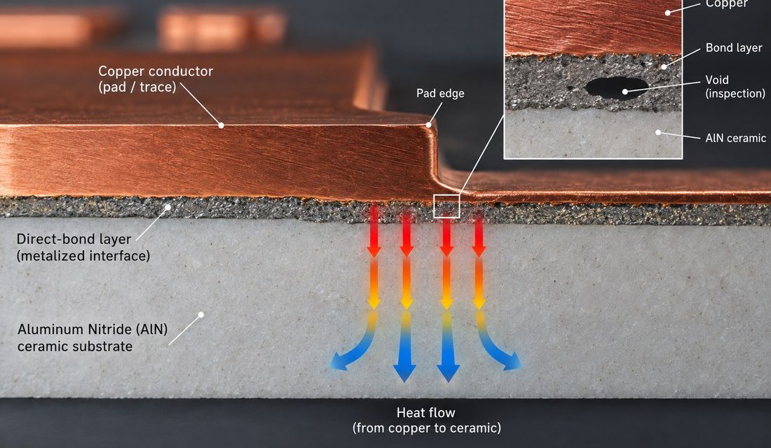
An Aluminum Nitride PCB direct-bond copper release needs a controlled metallization edge, via transition, and inspection record before qualification. Direct-bond copper can deliver a low-resistance thermal and electrical interface on aluminum nitride, but its edge, adhesion, and transition features must survive the same thermal history as the product. A qualification coupon that omits the heavy...
Alumina PCB DFM: Metallization, Panel Handling, and Inspection Before Volume Release

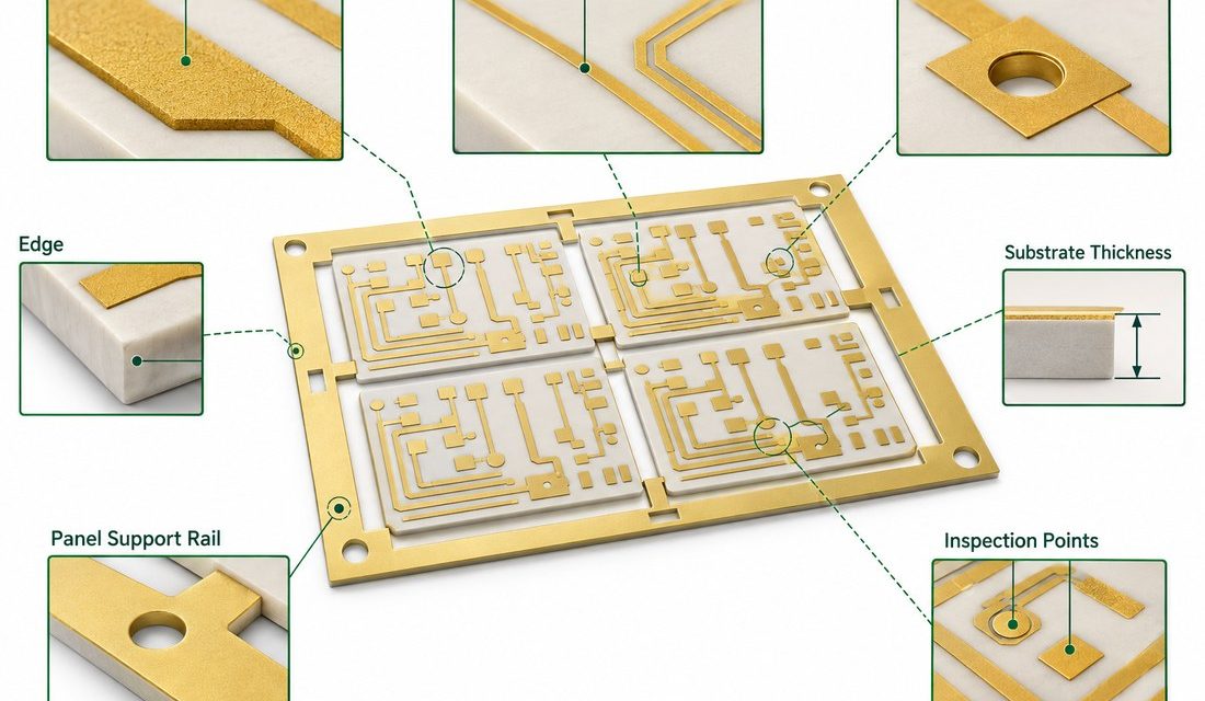
Volume release exposes the difference between a ceramic layout and a ceramic process. Screen, thick-film, thin-film, plated, brazed, and bonded features each have a different capability window. An Alumina PCB drawing that specifies only line widths and hole sizes can still leave the supplier guessing about paste, firing, edge handling, carrier support, and inspection. The...

Ceramic PCB Metallization and Via Reliability: A Practical Review for RF Power Boards

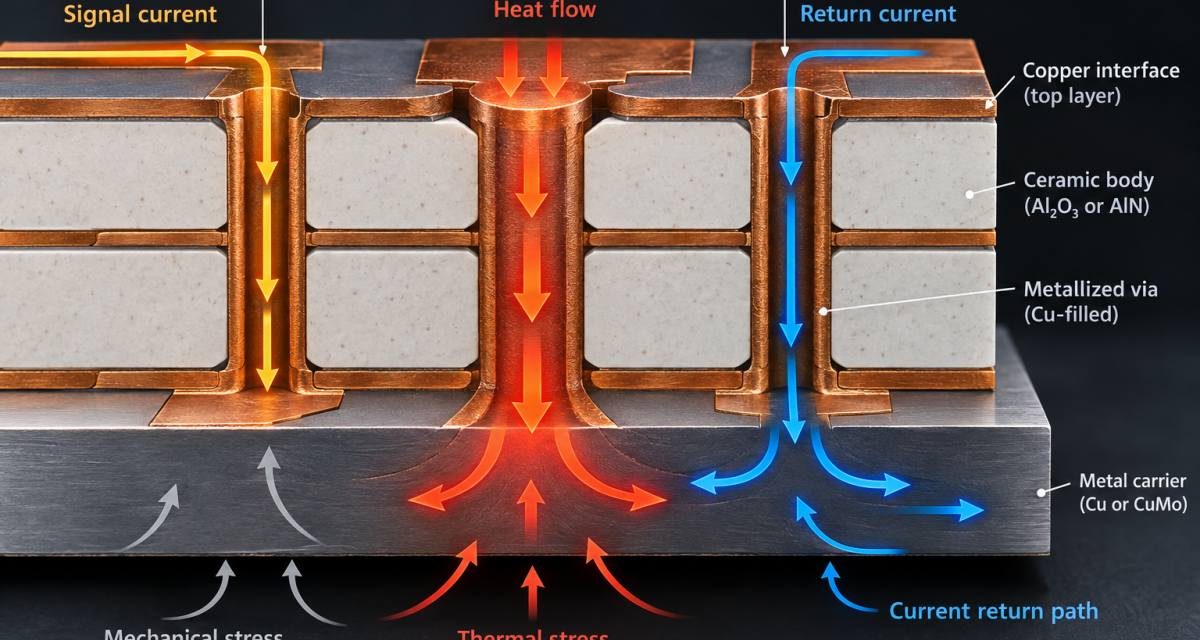
A ceramic substrate can be electrically stable and thermally efficient while the interconnect still becomes the weak point. Metallization adhesion, plated or filled vias, copper thickness, and the transition to a connector or carrier all experience different mechanical strain. For a Ceramic PCB used in a power or microwave module, the correct question is not...