Impedance Controlled PCB - KKPCB
 
HomeTag

Impedance Controlled PCB - KKPCB

Megtron 7 PCB: Ultra-Low Loss High-Speed PCBs for Advanced Digital and RF Systems

What Is a Megtron 7 PCB? A Megtron 7 PCB is a high-performance printed circuit board built using Panasonic Megtron 7 laminate, developed for ultra-high-speed digital and high-frequency signal transmission. Megtron 7 PCBs are widely used where signal integrity, extremely low transmission loss, and stable impedance control are critical, such as 5G routers, data-center equipment,...

RF-35 PCB: Cost-Effective Low-Loss High-Frequency PCBs for RF Applications

What Is an RF-35 PCB? An RF-35 PCB is a high-frequency printed circuit board fabricated using Taconic RF-35 laminate, specifically designed for RF, microwave, and high-speed signal transmission applications. RF-35 PCB material provides low dielectric loss, stable electrical performance, and good thermal reliability, making it a popular choice for RF Test PCB, communication equipment, and...

RO4350B PCB: Low-Loss High-Frequency PCBs Based on Rogers RO4350B

What Is an RO4350B PCB? An RO4350B PCB is a high-frequency printed circuit board fabricated with Rogers RO4350B laminate, designed for RF, microwave, and high-speed signal transmission. RO4350B combines low dielectric loss, stable dielectric constant, and FR-4–like manufacturability, making it one of the most widely used materials for RF and 5G applications. Key Material Properties...
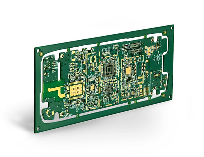
Impedance Controlled PCB: High-Speed and RF PCBs for Signal Integrity

What Is an Impedance Controlled PCB? An Impedance Controlled PCB is a printed circuit board designed with precisely engineered impedance values for high-speed or high-frequency signal paths. These PCBs ensure signal integrity, minimal reflection, and low insertion loss, which are critical for RF modules, 5G routers, high-speed digital circuits, automotive electronics, and sensor interfaces. Key...

High Frequency Sensor PCB: Precision PCBs for RF and High-Speed Sensor Applications

What Is a High Frequency Sensor PCB? A High Frequency Sensor PCB is a specialized printed circuit board engineered for high-frequency signal processing in sensors, such as radar, LiDAR, mmWave, and RF sensing modules. These PCBs are designed to maintain signal integrity, minimize insertion loss, and provide accurate impedance control, which are critical for precise...

Controlled Impedance PCB Prototype: Reducing Risk in High-Speed and RF Design Validation

For high-speed digital and RF electronic systems, signal integrity is one of the most critical design challenges. A controlled impedance PCB prototype plays a key role in validating design assumptions, manufacturing tolerances, and electrical performance before moving into mass production. Building controlled impedance into the prototype stage significantly reduces technical and production risk. What Is...

Controlled Impedance PCB Prototype: Accurate Signal Integrity Validation from Design to Production

As data rates and operating frequencies continue to increase, maintaining signal integrity becomes a critical design challenge. A controlled impedance PCB prototype allows engineers to verify impedance accuracy, minimize signal reflection, and validate high-speed or RF performance before entering mass production. By prototyping controlled impedance PCBs early, design risks are reduced and product reliability is...

Controlled Impedance PCB Prototype: Ensuring Signal Integrity in High-Speed and RF Designs

As digital speeds and operating frequencies continue to increase, maintaining signal integrity has become one of the biggest challenges in PCB design. A controlled impedance PCB prototype is a critical step in validating transmission line performance before mass production. By accurately controlling impedance during prototyping, engineers can reduce signal reflection, minimize loss, and ensure stable...

From Stackup Planning to Lamination Control: Engineering High Layer Count PCBs That Actually Work

Engineering High Layer Count PCBs: Why “More Layers” Isn’t the Answer As electronic systems evolve toward higher speeds, higher integration, and smaller form factors, high layer count PCBs—typically 16 layers and above—have become standard in data centers, telecommunications, aerospace electronics, and advanced industrial systems. However, many multilayer PCBs fail not because of schematic errors, but...

Achieve Ultra-Consistent Dk/Df Stability Using RO4835 PCB Architectures for High-Density 5G Massive-MIMO Radio Units

Next-generation 5G massive-MIMO radio units require high-density PCB designs that maintain ultra-consistent dielectric constant (Dk) and dissipation factor (Df) across all layers. Any variation in Dk/Df can lead to impedance mismatches, phase errors, and RF signal degradation, negatively affecting beamforming accuracy and spectral efficiency. RO4835 PCB laminates (Dk = 3.48 ± 0.03, Df = 0.0037...