
In an aircraft or spacecraft avionics bay, a connector is not merely a mechanical boundary. It is where fast edge currents, cable shields, PCB reference planes, enclosure metal, and installation tolerances meet.
A board can pass a schematic review yet radiate or pick up interference after integration because the signal return is forced through a long detour, the backshell bond is interrupted by paint or a gasket, or a shield termination is converted into a narrow pigtail. This Aerospace PCB design note focuses on the connector field: how to keep the high-frequency return geometry deliberate without confusing signal ground with chassis bonding. For an Aerospace PCB release, assign one owner to reconcile the board-edge datum, cable shield termination, and enclosure bond before the interface drawing is frozen. For this Aerospace PCB connector boundary, keep signal, return, shield, and chassis paths as separate review items.
For an Aerospace PCB release, start with the actual interface-control drawing, connector part family, backshell, cable shield construction, enclosure finish, and mounting hardware—not a generic “ground everything” rule. This Aerospace PCB interface definition should name the electrical and mechanical owners responsible for resolving any disagreement. Coordinate the board package with Aerospace PCB and the mechanical envelope early enough that connector datum, ground pins, fasteners, and keep-outs can be reviewed together.
In this article: define the interface · preserve the return path · separate shield and signal grounding · make the transition manufacturable · verify the assembled boundary
Treat the connector field as an electrical interface, not a footprint
Connector selection is only the beginning. The engineering definition should show board-edge or panel connector position, shell contact surfaces, PCB reference layers, shield termination, enclosure bond, mounting datum, and the signal pins that carry fast edges.
When multiple interfaces share an edge, establish pin-group ownership and reserve ground contacts adjacent to critical pairs where the connector architecture allows. Confirm the actual mating orientation and service access; a connector rotated for wrench clearance can move the return-via pair away from the launch and change the current loop. An Aerospace PCB launch review should therefore include the installed connector and enclosure, not only the bare-board footprint.
A practical interface review draws three paths independently: the intended differential or single-ended signal path; its local PCB return path; and the cable-shield/chassis path. Their physical intersections are deliberate connections, not assumptions. An Aerospace PCB connector-field review should record each intentional bond and the evidence that will verify it, rather than leaving the assembly team to infer the current path. For an Aerospace PCB review, confirm whether the proposed board edge, plating, via field, and mechanical tolerances can be fabricated and inspected as drawn.
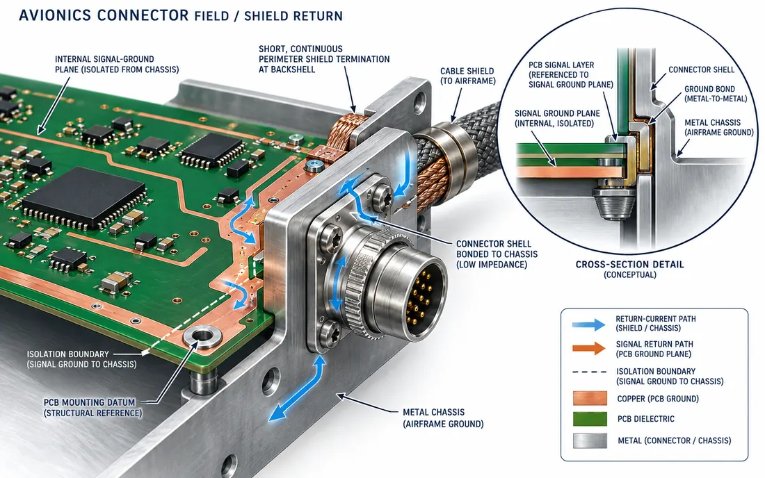
Keep the signal return local through the launch
At the board connector, a signal trace does not travel alone: its return current follows the lowest-impedance available path, which is shaped by the reference plane and discontinuities.
If the signal changes layers near the launch, place the return transition close enough to provide a continuous path, subject to the connector footprint, drill rules, and the actual layer reference. A ground via placed “nearby” in a visual sense may still be electrically remote when a connector pin, anti-pad, plane void, or split interrupts the path. On an Aerospace PCB, include the mating connector and enclosure boundary in that review; a board-only view can hide the return discontinuity created by the installed hardware.
Review the cross-section and top view together. Check the launch pad and neck-down, differential-pair symmetry, antipad geometry, reference-plane continuity, return-via location, solder-mask definition, and connector keep-out. Avoid a plane split under the launch simply to clear a mounting feature; instead compare alternate layer assignments or a controlled local cutout whose effect is assessed in the field solver or measurement plan. For an Aerospace PCB section, the transition should be evaluated as a three-dimensional discontinuity rather than judged only by nominal trace impedance.
A representative design exercise—not a KKPCB measurement—can compare two candidate launch layouts in a 3D EM model using the connector vendor’s footprint, the actual laminate construction, copper thickness, and enclosure boundary. Sweep the intended band and include plausible manufacturing variation in pad, drill, and registration dimensions.
The decision metric may include return loss, insertion loss, mode conversion, and phase mismatch, but those limits must come from the system link budget and interface specification. Do not transfer a number from a different connector, stackup, or test fixture.
Do not substitute a signal-ground pin for a shield bond
NASA’s spacecraft grounding guidance describes peripheral, low-impedance shield termination through the backshell and connector-to-mounting interface as the preferred approach for the cable shield. That is a system-level EMC recommendation, not a universal instruction to short every PCB signal plane directly to the enclosure.
The architecture must distinguish the overshield or cable braid, connector shell, chassis, PCB signal reference, and any isolated circuit domain. A pin that carries the shield through the enclosure and grounds it only inside the box can compromise the enclosure boundary; a long drain-wire pigtail adds inductance and can be ineffective at higher frequencies.
Where a low-frequency ground-loop concern competes with high-frequency shielding, resolve it at the equipment and harness architecture level with the EMC/system engineer. Do not make an ad hoc one-end-open shield choice on the PCB drawing. The Aerospace PCB shield strategy belongs to the equipment-and-harness definition, with the board drawing showing the resulting interface rather than inventing it locally. Record the selected bond topology, expected current paths, finish/contact requirements, and verification method in the interface-control and assembly documents. A PCB Assembly package should make connector-shell soldering, hardware installation, and inspection points unambiguous.
On the board, define which ground pins connect to the local reference plane and which metal features bond to chassis. If a capacitor or RC network is part of an intentional EMC strategy, document its voltage rating, pulse/current stress, placement, and failure behavior; do not treat it as a generic substitute for a mechanically reliable metal bond. Keep chassis current away from quiet sensor returns and sensitive analog reference nodes unless the system grounding plan explicitly routes them together.
When edge treatment, conductive contact land, or via placement changes during development, keep the Aerospace PCB fabrication drawing and the electrical interface definition synchronized; otherwise, a mechanical revision can silently invalidate the return-path review.
Design the bond so fabrication and assembly can preserve it
A good drawing can still become a poor interface if the production package leaves contact details implicit. Specify whether exposed copper, plated contact lands, conductive finish, or a separate bonding feature is required; identify surfaces that must remain free of solder mask, coating, adhesive, or paint; and show the hardware stack-up, washer, fastener, torque source, and inspection access where relevant. The requirements must follow the customer’s drawing and governing standard. Do not add an arbitrary bond-resistance acceptance value without the project authority defining test points, current, probe method, and limit.
Ask fabrication to review copper-to-edge clearance, edge plating feasibility, connector-hole tolerances, drill-to-copper registration, and whether the selected surface finish is compatible with the contact design.
A PCB fabrication capability check belongs before the package is frozen. Aerospace PCB manufacturing release should state which edge and contact features require inspection. For an Aerospace PCB connector zone, make exposed-contact, edge-plating, and mask-clearance requirements explicit on the controlled fabrication data. For a dense connector zone, HDI PCB structures may help route escape fanout, but via-in-pad, stacked microvias, and filled/plated via details must be agreed against reliability, inspection, and supplier capability—not selected solely to recover routing space.
Prototype builds are useful for discovering tool access, connector insertion direction, mating clearance, and rework constraints before an expensive environmental qualification unit is assembled. A PCB prototype assembly stage should preserve the intended connector, backshell, fasteners, and cable representative enough to expose interface issues; a bare-board coupon alone cannot reveal enclosure access or harness strain.
Verify the assembled boundary, not only the bare board
Plan evidence at multiple levels. During design review, confirm the return path through every signal-layer change and check the connector-field 3D model against the intended enclosure. During fabrication acceptance, inspect the board-edge geometry, plated features, mask openings, and registration called out on the drawing. During assembly, verify shell seating, fastener access, contact surfaces, cable shield termination, and that a coating or gasket has not been introduced across a required bond.
For conducted and radiated EMC work, agree the harness configuration, enclosure state, cable routing, terminations, grounding points, and test setup before measuring.
A result without those conditions is difficult to reproduce and may not represent the integrated product. An Aerospace PCB qualification record should preserve the exact connector and harness configuration used for each result. An Aerospace PCB qualification plan should lock the connector, backshell, cable, enclosure, and bond hardware configuration before test dates are committed. If qualification is planned, make a representative assembly and fixture plan part of the project schedule; connector and cable substitutions should trigger impact review because they change the electrical boundary.
When the interface must flex or packaging is unusually constrained, review whether a rigid-flex PCB or a separate interconnect architecture is more appropriate. Mechanical bend zones should not cross the connector launch or a required shield-bond land. If that architecture proceeds, rigid-flex assembly details need an explicit bend, stiffener, and inspection definition rather than a generic outline note.
At program level, keep the Aerospace PCB interface tied to the approved avionics ICD, harness definition, enclosure drawing, and configuration index.
Release checklist for the avionics connector boundary
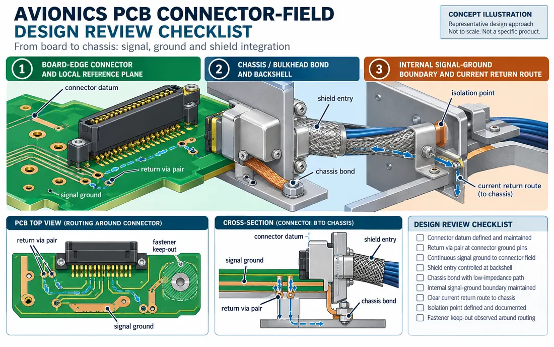
- Identify connector, backshell, cable shield, enclosure, finish, and mating hardware by controlled part/drawing revision.
- Show signal, PCB reference, shield, and chassis paths separately, including all layer transitions and intentional bonds.
- Place return vias and reference-plane transitions based on launch geometry and the selected verification method.
- Define contact land, mask/coating exclusions, edge treatment, mechanical datum, keep-outs, and inspection access.
- Validate the assembled connector and harness boundary in the relevant simulation, inspection, and EMC test configuration.
- Review substitutions and drawing changes for impact on launch geometry, shield continuity, bond surfaces, and qualification evidence.
A project handoff may include an SMT assembly plan for board-side parts and a separate through-hole assembly definition for connector hardware where applicable.
If a cable harness or board revision changes late, use documented PCB manufacturing change control to preserve the approved interface and traveler evidence. For specialized controlled-impedance sections near the connector, consult the high-frequency PCB capability scope before finalizing a stackup assumption. For early engineering builds, an unlinked prototype build can expose assembly access issues before qualification, while final procurement should keep the approved configuration and inspection record aligned with controlled production documentation.
Sources: NASA-HDBK-4001A, Electrical Grounding Architecture for Unmanned Spacecraft (2025), particularly the guidance on shield termination through connector backshells and enclosure interfaces; NASA-STD-4003A, Electrical Bonding for NASA Launch Vehicles, Spacecraft, Payloads, and Flight Equipment. Apply the governing project revision and requirements; this article is an engineering design discussion, not a substitute for the project’s EMC authority, approved drawings, or qualification plan.


