
HomeTag

IC Burn-in Board - KKPCB

Burn-in PCB – High Reliability Test Boards for IC Burn-in and Stress Testing

What Is a Burn-in PCB? A Burn-in PCB is a specialized printed circuit board designed for semiconductor burn-in testing. It is used to apply electrical and thermal stress to integrated circuits (ICs) over an extended period to identify early-life failures and ensure long-term reliability. Burn-in testing is a critical quality control process in semiconductor manufacturing,...
Burn-in Board PCB for Semiconductor Reliability and Stress Testing

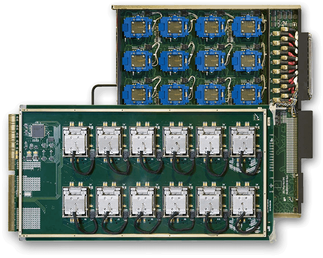
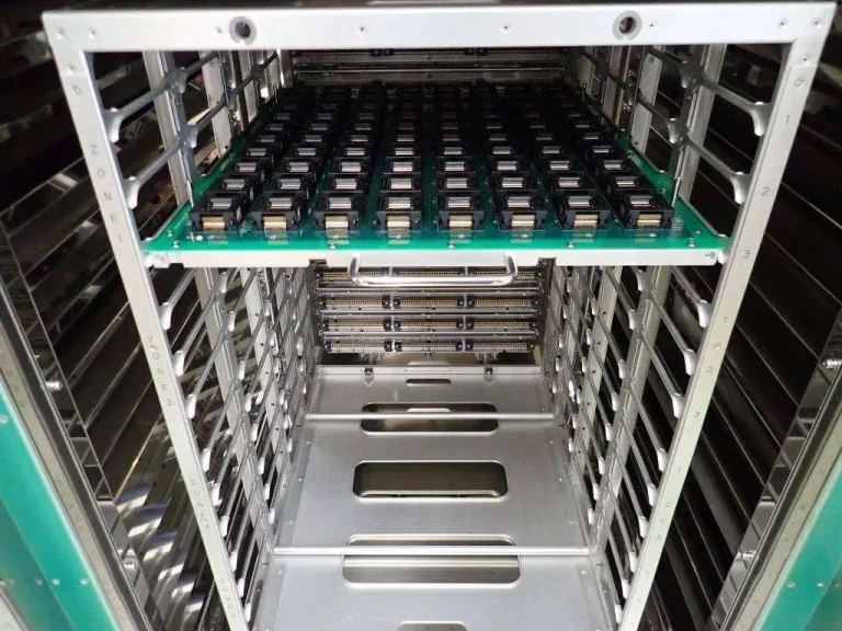
What Is a Burn-in Board PCB? A Burn-in Board PCB is a specialized printed circuit board used in semiconductor reliability testing to identify early device failures. It connects packaged integrated circuits to burn-in test systems, allowing devices to operate under elevated temperature, voltage, and electrical stress conditions over extended periods. Burn-in board PCBs play a...

Burn-in Board PCB: High-Reliability PCB Solutions for Semiconductor Burn-In Testing

The Role of Burn-in Board PCB in Semiconductor Testing In semiconductor manufacturing, reliability screening is essential to identify early-life failures before products reach end customers. A Burn-in Board PCB is a specialized semiconductor test PCB designed to operate under elevated temperatures, continuous electrical stress, and extended test durations to evaluate device reliability. Installed inside burn-in...