
The Role of Burn-in Board PCB in Semiconductor Testing
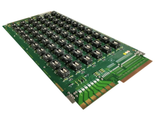
In semiconductor manufacturing, reliability screening is essential to identify early-life failures before products reach end customers. A Burn-in Board PCB is a specialized semiconductor test PCB designed to operate under elevated temperatures, continuous electrical stress, and extended test durations to evaluate device reliability.
Installed inside burn-in ovens or Automated Test Equipment (ATE) systems, burn-in board PCBs provide the electrical interface between semiconductor devices and test systems, ensuring stable power delivery, accurate monitoring, and consistent stress conditions throughout the testing process.
Compared with conventional IC test boards, burn-in board PCBs require higher levels of:
- Thermal stability
- Electrical reliability
- Mechanical durability
- Long-term operational consistency
A well-engineered burn-in board ensures accurate failure screening and improves semiconductor quality and production yield.
Key Design Requirements of Burn-in Board PCBs
1. High-Temperature Material Stability
Burn-in testing exposes PCBs to prolonged high-temperature environments, making material reliability a critical factor.
High-quality burn-in board PCBs typically require:
- High-Tg laminate materials
- Low thermal expansion characteristics
- Stable dielectric properties
- Resistance to thermal aging
Proper material selection helps prevent:
- PCB warpage
- Layer delamination
- Dielectric degradation
- Electrical performance drift
Maintaining material stability ensures reliable operation throughout repeated burn-in cycles.
2. Robust Power Delivery and Current Handling
During burn-in testing, semiconductor devices often operate under continuous electrical stress. The PCB must provide stable power distribution while handling increased current loads.
Important design considerations include:
- Optimized power and ground planes
- Adequate copper thickness
- Reinforced via structures
- Low-resistance current paths
- Effective thermal management
A reliable power delivery network prevents voltage fluctuation and ensures consistent device stress conditions during testing.
3. Controlled Impedance and Signal Integrity
Although burn-in testing focuses primarily on reliability screening, monitoring and control signals still require stable electrical performance.
Controlled impedance design helps maintain:
- Reliable communication between DUTs and test systems
- Reduced signal distortion
- Stable monitoring accuracy
Key factors include:
- Proper stack-up design
- Consistent trace geometry
- Controlled dielectric thickness
- Reference plane optimization
These measures ensure reliable signal transmission even under thermal stress.
4. Mechanical Durability and Socket Reliability
Burn-in boards typically experience repeated device insertion, removal, and thermal cycling.
Mechanical reliability requirements include:
- Excellent PCB flatness
- Stable dimensional control
- Reinforced socket mounting areas
- Reliable contact alignment
A mechanically robust burn-in board minimizes:
- Socket contact failures
- Mechanical deformation
- Test interruptions
This improves overall test efficiency and repeatability.
5. Long-Term Electrical Reliability
Burn-in testing may continue for hours or even days under continuous operation. Therefore, the PCB must maintain stable electrical characteristics over extended periods.
Critical requirements include:
- Low electrical drift
- Reliable interconnect structures
- Durable surface finishes
- Consistent manufacturing quality
Long-term electrical stability ensures accurate identification of early semiconductor failures.
Applications of Burn-in Board PCBs
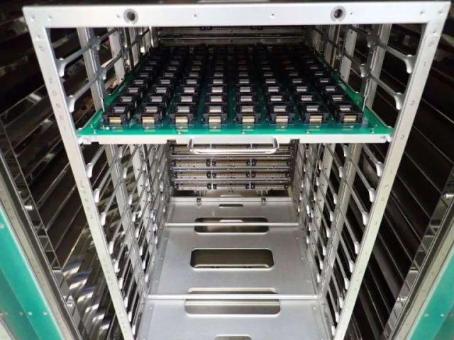
Burn-in Board PCBs are widely used in semiconductor reliability testing, including:
- Logic IC burn-in testing
- Memory burn-in testing for DRAM, NAND, and Flash devices
- Automotive-grade semiconductor qualification
- Industrial and high-reliability electronics testing
- Aerospace and defense semiconductor screening
- Production quality assurance processes
These applications require consistent electrical performance and long-term reliability under demanding conditions.
Manufacturing Requirements for Reliable Burn-in Board PCBs
Producing high-performance burn-in boards requires specialized PCB manufacturing capabilities, including:
High-Temperature PCB Processing
- High-Tg laminate fabrication
- Thermal stress resistance control
- Stable multilayer construction
Power and Reliability Optimization
- Heavy copper power structures
- Reliable via plating
- Optimized thermal management
Precision Manufacturing Control
- Accurate layer registration
- Controlled impedance fabrication
- Reliable surface finishing
- Electrical performance verification
Flexible Production Support
- Prototype development
- Small-batch production
- Volume manufacturing
These capabilities ensure consistent performance throughout repeated burn-in cycles.
Why Burn-in Board PCB Quality Matters
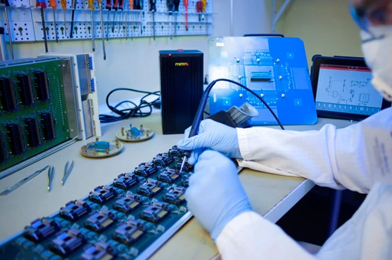
Poor-quality burn-in boards can introduce additional risks, including:
- False failure detection
- Unstable test conditions
- Reduced screening accuracy
- Increased maintenance and replacement costs
A high-quality Burn-in Board PCB provides:
- Accurate early-life failure identification
- Stable performance under high-temperature stress
- Longer service life
- Improved semiconductor reliability
- Reduced overall testing costs
Conclusion: Supporting Reliable Semiconductor Qualification
The Burn-in Board PCB is a critical component in semiconductor reliability testing, enabling devices to be screened under controlled thermal and electrical stress conditions.
Through high-temperature material selection, robust power design, controlled impedance routing, and precision manufacturing processes, reliable burn-in board PCBs help semiconductor manufacturers achieve accurate failure detection, improved production yield, and higher product reliability.
Partnering with an experienced Burn-in Board PCB manufacturer ensures consistent quality and dependable performance throughout the semiconductor testing lifecycle.

